SO-502 SAW Based Oscillator
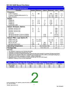
Vcc - 1.0V
Vcc - 1.3V
Vcc - 1.6V
80%
20%
tB
Figure 1. 100K PECL Waveform
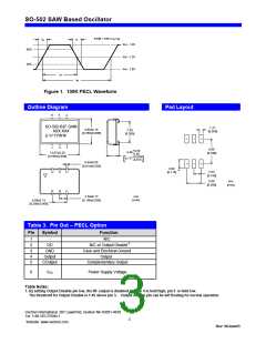
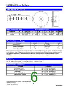
Outline Diagram
Pad Layout
6
5
4
VS-500-LFF-GNN
SO-502-BJF-GNN
1.27
8.89±0.15
7.63
[0.300]
XXX.XXX
XXX.XXX
[0.050]
[0.350±0.006]
VI YWW
∆ VI YYWW
3
1
2
8.80
+0.20
4.49
13.97±0.20
[0.550±0.008]
[0.346]
-0.30
+0.008
-0.012
0.177
[
]
0.46±0.05
[0.018±0.002]
3.00
2.54
[0.118]
[0.100]
5.08
mm
[0.200]
[inch]
2.54±0.13
[0.100±0.005]
mm
[inch]
5.08±0.13
[0.200±0.005]
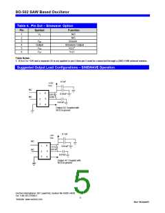
Table 3. Pin Out – PECL Option
Pin
Symbol
Function
N/C
1
2
3
4
5
-
N/C or Output Disable1
Case and Electrical Ground
Output
OD
GND
Output
COutput
Complementary Output
6
VCC
Power Supply Voltage
Table Notes:
1. By setting Output Disable pin low, the RF output is disabled and pin 4 is held high, pin 5 is held low.
The threshold for Output Disable is 1.4V above pin 3. Output disable pin can be left floating for normal operation
Vectron International, 267 Lowell Rd, Hudson NH 03051-4916
Tel: 1-88-VECTRON-1
Website: www.vectron.com
3
Rev: 06June05

 VECTRON [ Vectron International, Inc ]