4N65
Power MOSFET
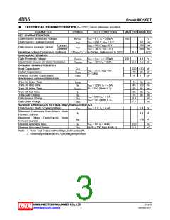
ELECTRICAL CHARACTERISTICS (TC =25°С, unless otherwise specified)
PARAMETER
SYMBOL
TEST CONDITIONS
MIN TYP MAX UNIT
OFF CHARACTERISTICS
Drain-Source Breakdown Voltage
Drain-Source Leakage Current
BVDSS
IDSS
VGS = 0 V, ID = 250μA
650
V
VDS = 650 V, VGS = 0 V
VGS = 30 V, VDS = 0 V
10
μA
Forward
Reverse
100 nA
-100 nA
V/°С
Gate-Source Leakage Current
IGSS
VGS = -30 V, VDS = 0 V
ID=250μA, Referenced to 25°C
△BVDSS/△TJ
Breakdown Voltage Temperature Coefficient
ON CHARACTERISTICS
Gate Threshold Voltage
Static Drain-Source On-State Resistance
DYNAMIC CHARACTERISTICS
Input Capacitance
0.6
VGS(TH)
RDS(ON)
VDS = VGS, ID = 250μA
2.0
4.0
2.4 2.5
V
VGS = 10 V, ID = 2.2A
Ω
CISS
COSS
CRSS
520 670 pF
VDS = 25 V, VGS = 0V,
f = 1MHz
Output Capacitance
70
8
90
11
pF
pF
Reverse Transfer Capacitance
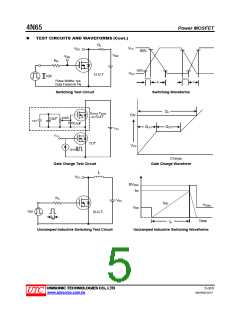
SWITCHING CHARACTERISTICS
Turn-On Delay Time
tD(ON)
tR
tD(OFF)
tF
13
35
ns
Turn-On Rise Time
45 100 ns
VDD = 325V, ID = 4.0A,
RG = 25Ω (Note 1, 2)
Turn-Off Delay Time
25
35
60
80
20
ns
ns
Turn-Off Fall Time
Total Gate Charge
QG
15
nC
nC
nC
VDS= 520V,ID= 4.0A,
Gate-Source Charge
QGS
QGD
3.4
7.1
VGS= 10V (Note 1, 2)
Gate-Drain Charge
SOURCE- DRAIN DIODE RATINGS AND CHARACTERISTICS
Drain-Source Diode Forward Voltage
Maximum Continuous Drain-Source Diode
Forward Current
VSD
VGS = 0 V, IS = 4.4A
1.4
4.4
V
A
IS
Maximum Pulsed Drain-Source Diode
Forward Current
ISM
17.6
A
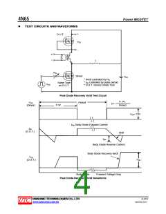
Reverse Recovery Time
trr
250
1.5
ns
V
GS = 0V, IS = 4.4A,
dIF/dt = 100 A/μs (Note 1)
Reverse Recovery Charge
QRR
μC
Note: 1. Pulse Test: Pulse width≤300μs, Duty cycle≤2%
2. Essentially independent of operating temperature
UNISONIC TECHNOLOGIES CO., LTD
3 of 8
QW-R502-397.F
www.unisonic.com.tw

 UTC [ Unisonic Technologies ]