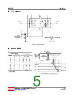
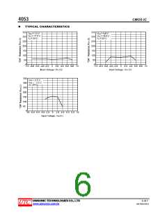
4053
CMOS IC
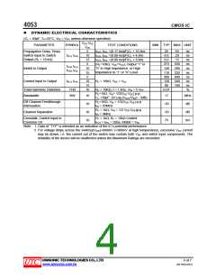
DYNAMIC ELECTRICAL CHARACTERISTICS
(CL = 50pF, TA=25°C, VEE≦VSS, unless otherwise specified)
V
DD-VEE
VDC
5
PARAMETER
SYMBOL
tPLH, tPHL
TEST CONDITIONS
MIN TYP MAX UNIT
tPLH, tPHL =(0.17 ns/pF)CL + 16.5ns
tPLH, tPHL =(0.08 ns/pF)CL + 4.0ns
tPLH, tPHL =(0.06 ns/pF)CL + 3.0ns
25
8.0
65
20
ns
ns
ns
ns
ns
ns
ns
ns
ns
%
Propagation Delay Times
Switch Input to Switch
Output (RL = 10 kΩ)
10
15
6.0
15
5
275
140
110
300
120
80
550
280
220
600
240
160
(RL=10kΩ, VEE=VSS), Output “1” or
“0” to High Impedance, or High
Impedance to “1” or “0” Level
t
t
PHZ, tPLZ
PZH, tPZL
Inhibit to Output
10
15
5
Control Input to Output
tPLH, tPHL
10
15
10
RL = 10kΩ, VEE = VSS
Total Harmonic Distortion
Bandwidth
THD
BW
RL = 10KΩ, f = 1 kHz, VIN = 5 VPP
RL=1kΩ, VIN= 1/2(VDD-VEE) p-p,
CL =50pF, 20 Log (VOUT/VIN)= -3dB)
RL=1KΩ, VIN = 1/2(VDD-VEE) p-p
IN = 55MHz
RL = 1kΩ, VIN = 1/2 VDD-VEE)p-p
IN = 3MHz
R1 = 1kΩ, RL = 10kΩ Control
TLH = tTHL = 20ns, Inhibit = VSS
0.07
10
10
10
10
17
-50
-50
75
MHz
dB
Off Channel Feedthrough
Attenuation
f
Channel Separation
dB
f
Crosstalk, Control Input to
Common O/I
mV
t
Note: 1. Data of “TYP” is intended as an indication of the IC’s potential performance.
2. For voltage drops across the switch(ΔVSW)>600mV (>300mV at high temperature), excessive VDD current
may be drawn, i.e. the current out of the switch may contain both VDD and switch input components. The
reliability of the device will be unaffected unless the Maximum Ratings are exceeded.
UNISONIC TECHNOLOGIES CO., LTD
4 of 7
QW-R502-036.D
www.unisonic.com.tw

 UTC [ Unisonic Technologies ]