4053
CMOS IC
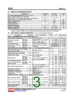
ABSOLUTE MAXIMUM RATING
PARAMETER
SYMBOL
VDD
RATINGS
-0.5 ~ +18
UNIT
V
DC Supply Voltage (Referenced to VEE, VSS≧VEE
)
Input or Output Voltage (DC or Transient)
VIN, VOUT
-0.5 ~ VDD +0.5
V
(Referenced to VSS for Control Inputs and VEE for Switch I/O)
Input Current (DC or Transient), per Control Pin
Switch Through Current
IIN
±10
±25
mA
mA
ISW
Power Dissipation
500
mW
mW/°C
°C
PD
Derating above 65°C
7
Junction Temperature
TJ
125
Operating Temperature
TOPR
TSTG
-40 ~ +125
-40 ~ +150
°C
Storage Temperature
°C
Note: Absolute maximum ratings are those values beyond which the device could be permanently damaged.
Absolute maximum ratings are stress ratings only and functional device operation is not implied.
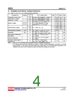
ELECTRICAL CHARACTERISTICS (TA=25°C, unless otherwise specified.)
PARAMETER
SYMBOL
TEST CONDITIONS
MIN
TYP
MAX UNIT
SUPPLY REQUIREMENTS (Voltages Referenced to VEE
)
VDD – 3≧VSS≧VEE
Power Supply Voltage Range
VDD
IQ
3
18
5
V
VDD=5V
0.005
0.010
0.015
µA
µA
µA
µA
µA
µA
Control Inputs: VIN = VSS or VDD
Switch I/O: VEE ≦VI/O ≦VDD
ΔVSW≦500mV (Note 2)
Quiescent Current per
Package
,
VDD=10V
VDD=15V
10
20
V
DD=5V
(0.07 µA/kHz) f + IQ
(0.20 µA/kHz) f + IQ
(0.36 µA/kHz) f + IQ
)
Total Supply Current
TA=25°C only (The channel
ID(AV) component, (VIN-VOUT)/RON, is
excluded)
(Dynamic Plus Quiescent, VDD=10V
Per Package)
VDD=15V
SWITCHES IN/OUT AND COMMONS OUT/IN -- X, Y, Z (Voltages Referenced to VEE
Recommended Peak–to–Peak Voltage
Into or Out of the Switch
VI/O
Channel On or Off
0
VDD
600
VPP
mV
Recommended Static or Dynamic
Voltage Across the Switch (Note2)
Output Offset Voltage
ΔVSW Channel On
0
VO(OFF) VIN = 0V, No Load
10
250
120
80
µV
Ω
Ω
Ω
Ω
Ω
Ω
ΔVSW≦500mV
VDD=5V
1050
500
280
70
ON Resistance
VDD=10V
VDD=15V
VDD=5V
VDD=10V
VDD=15V
RON
ΔRON
IOFF
VIN = VIL or VIH (Control), and
IN = 0 to VDD (Switch)
V
ΔON Resistance Between
Any Two Channels in the
Same Package
25
10
50
10
45
VIN = VIL or VIH (Control)
Channel to Channel or Any One
Channel, VDD=15V
Inhibit = VDD
Off–Channel Leakage Current
±0.05
±100 nA
Capacitance, Switch I/O
Capacitance, Common O/I
Capacitance, Feedthrough
(Channel Off)
CI/O
CO/I
10
17
pF
pF
pF
Pf
Inhibit = VDD
Pins Not Adjacent
Pins Adjacent
0.15
0.47
CI/O
CONTROL INPUTS – INHIBIT A, B, C (Voltages Referenced to VSS
DD=5V
)
V
2.25
4.50
6.75
2.75
5.50
8.25
1.5
3.0
4.0
V
V
Low Level Input Voltage
VDD=10V
VDD=15V
VIL
RON= per spec, IOFF = per spec
V
VDD=5V
3.5
7.0
11
V
High Level Input Voltage
VDD=10V
VDD=15V
VIH
RON= per spec, IOFF = per spec
V
V
Input Leakage Current
Input Capacitance
ILEAK VIN= 0 or VDD, VDD=15V
CIN
±0.00001 ±0.1
5.0 7.5
µA
pF
UNISONIC TECHNOLOGIES CO., LTD
3 of 7
QW-R502-036.D
www.unisonic.com.tw

 UTC [ Unisonic Technologies ]