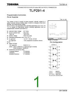
TLP291-4
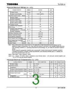
Absolute Maximum Ratings
(Ta = 25℃)
RATING
CHARACTERISTIC
SYMBOL
UNIT
Forward Current
I
50
mA
F(RMS)
Forward Current Derating
∆I /°C
F
−0.67 (Ta≥50°C)
mA /°C
Pulse Forward Current
Reverse Voltage
(Note2)
I
1
5
A
V
FP
V
R
Junction Temperature
Collector-Emitter Voltage
Emitter-Collector Voltage
Collector Current
T
125
80
7
°C
V
j
V
V
CEO
ECO
V
I
C
50
mA
Collector Power Dissipation
(1 Circuit)
P
C
100
mW
Collector Power Dissipation
∆P /°C
−1.0
mW /°C
C
Derating(Ta≥25°C)
(1 Circuit)
Junction Temperature
T
125
°C
°C
°C
°C
j
Operating Temperature Range
T
−55 to 110
−55 to 125
260 (10s)
opr
stg
Storage Temperature Range
T
Lead Soldering Temperature
T
sol
Total Package Power Dissipation
P
T
170
mW
(1 Circuit)
Total Package Power Dissipation
∆P /°C
−1.7
mW /°C
Vrms
T
Derating (Ta≥25°C)
(1 Circuit)
(Note3)
Isolation Voltage
BV
S
2500
Note: Using continuously under heavy loads (e.g. the application of high temperature/current/voltage and the
significant change in temperature, etc.) may cause this product to decrease in the reliability significantly even
if the operating conditions (i.e. operating temperature/current/voltage, etc.) are within the absolute maximum
ratings.
Please design the appropriate reliability upon reviewing the Toshiba Semiconductor Reliability Handbook
(“Handling Precautions”/“Derating Concept and Methods”) and individual reliability data (i.e. reliability test
report and estimated failure rate, etc).
Note2: Pulse width ꢁ 100μs, frequency 100Hz
Note3: AC, 1 minute, R.H.≤60%, Device considered a two terminal device : LED side pins shorted together and
DETECTOR side pins shorted together.
Individual Electrical Characteristics
(Ta = 25℃)
CHARACTERISTIC
Forward Voltage
SYMBOL
TEST CONDITION
= 10 mA
F
MIN
1.1
TYP.
MAX
UNIT
V
I
I
1.20
—
1.4
10
—
V
μA
pF
V
F
Reverse Current
V = 5 V
R
—
—
80
7
R
Capacitance
C
V = 0, f = 1 MHz
30
T
Collector-Emitter Breakdown Voltage
Emitter-Collector Breakdown Voltage
V
V
I
I
= 0.5 mA
= 0.1 mA
= 48 V,
—
—
(BR) CEO
(BR) ECO
C
E
V
—
—
V
V
0.01
0.1
μA
μA
—
—
CE
Collector Dark Current
(Note5)
I
CEO
= 48 V, Ta = 85°C
2
50
CE
Capacitance
(Collector to Emitter)
C
V = 0, f = 1 MHz
10
—
pF
—
CE
3
2011-09-08

 TOSHIBA [ TOSHIBA ]