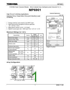
MP6901
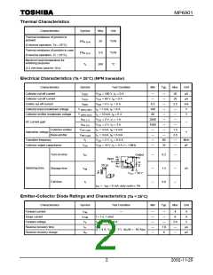
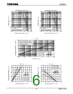
Thermal Characteristics
Characteristics
Symbol
Max
25
Unit
Thermal resistance of junction to
ambient
ΣR
°C/W
th (j-a)
th (j-c)
(6 devices operation, Ta = 25°C)
Thermal resistance of junction to case
(6 devices operation, Tc = 25°C)
ΣR
5.0
°C/W
°C
Maximum lead temperature for
soldering purposes
T
260
L
(3.2 mm from case for 10 s)
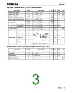
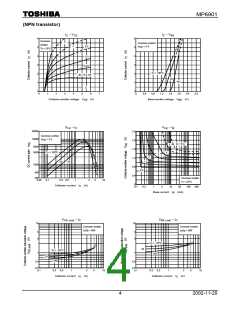
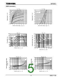
Electrical Characteristics (Ta = 25°C) (NPN transistor)
Characteristics
Symbol
Test Condition
= 100 V, I = 0 A
Min
Typ.
Max
Unit
Collector cut-off current
I
I
V
V
V
―
―
―
―
―
―
―
―
―
―
―
60
35
20
20
2.5
―
µA
µA
mA
V
CBO
CEO
CB
CE
EB
E
Collector cut-off current
= 80 V, I = 0 A
B
Emitter cut-off current
I
= 5 V, I = 0 A
0.5
100
80
EBO
C
Collector-base breakdown voltage
Collector-emitter breakdown voltage
V
V
I
I
= 1 mA, I = 0 A
E
(BR) CBO
(BR) CEO
C
C
= 10 mA, I = 0 A
―
V
B
h
h
V
V
= 2 V, I = 1 A
2000
1000
―
―
FE (1)
CE
CE
C
DC current gain
―
= 2 V, I = 3 A
―
FE (2)
C
Collector-emitter
Saturation voltage
V
I
I
= 3 mA, I = 6 mA
1.5
2.0
―
CE (sat)
BE (sat)
C
C
B
V
Base-emitter
V
= 3 mA, I = 6 mA
―
B
Transition frequency
f
V
V
= 2 V, I = 0.5 A
―
MHz
pF
T
CE
CB
C
Collector output capacitance
C
= 10 V, I = 0 A, f = 1 MHz
―
―
ob
E
Turn-on time
t
―
―
―
0.2
1.5
0.6
―
―
―
Output
on
I
I
B1
B2
Input
20 µs
Switching time
µs
Storage time
Fall time
t
stg
V
= 30 V
CC
t
f
I
= −I = 6 mA, duty cycle ≤ 1%
B2
B1
Emitter-Collector Diode Ratings and Characteristics (Ta = 25°C)
Characteristics
Forward current
Symbol
Test Condition
Min
Typ.
Max
Unit
I
―
―
―
―
―
―
―
―
―
1.0
8
4
6
A
A
FM
Surge current
I
t = 1 s, 1 shot
FSM
Forward voltage
V
I
= 1 A, I = 0 A
2.0
―
―
V
F
F
B
Reverse recovery time
Reverse recovery charge
t
µs
µC
rr
I
= 4 A, V = −3 V, dI /dt = −50 A/µs
F
BE
F
Q
rr
2
2002-11-20

 TOSHIBA [ TOSHIBA ]