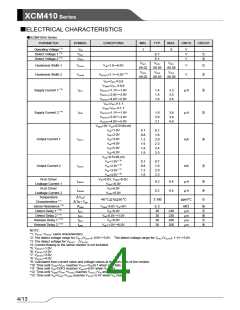
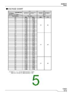
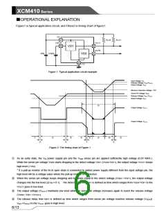
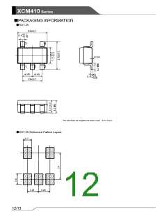
XCM410 Series
■NOTE ON USE
1. Use this IC within the stated maximum ratings. Operation beyond these limits may cause degrading or permanent
damage to the device.
2. The power supply input pin voltage drops by the resistance between power supply and the VIN pin, and by through current
at operation of the IC. At this time, the IC may go into malfunction if the power supply input pin voltage falls below the
minimum operating voltage range.
3. When the sense voltage is less than 1.0V, be sure to separate the VIN pin and the sense pin, and to apply the voltage over
1.0V to the VIN pin.
4. Note that a rapid and high fluctuation at the power supply input pin voltage may cause a wrong operation.
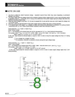
5. In N channel open drain output, VOUT voltages at detect and release are determined by resistance of a pull-up resistor
connected at the VOUT pin. Please choose proper resistance values with referring to Figure 3;
During detection:VOUT=Vpull / (1+Rpull / RON
)
Vpull:Pull-up voltage
RON(*1):On-resistance of N channel driver M3 can be calculated as VDS / IOUT1 from electrical characteristics,
For example, when (*2) RON = 0.5 / 0.8×10-3 = 625Ω(MIN.)at VIN=2.0V, Vpull = 3.0V and VOUT ≦0.1V at detect,
Rpull= (Vpull /VOUT-1)×RON= (3 / 0.1-1)×625≒18kΩ
In this case, Rpull should be selected higher or equal to 18kΩ in order to keep the output voltage less than 0.1V during
detection.
(*1)
V
is smaller RON is bigger, be noted.
IN
(*2) For calculation, minimum VIN should be chosen among the input voltage range.
During releasing:VOUT = Vpull / (1 + Rpull / ROFF
)
Vpull:Pull-up voltage
ROFF:On-resistance of N channel driver M3 is 15MΩ(MIN.)when the driver is off (as to VOUT / ILEAK)
For example:when Vpull = 6.0V and VOUT ≧ 5.99V,
Rpull = (Vpull / VOUT-1)×Roff = (6/5.99-1)×15×106 ≒25 kΩ
In this case, Rpull should be selected smaller or equal to 25 kΩ in order to obtain output voltage higher than 5.99V
during releasing.
NOTE: Roff=VOUT/ILEAK
Figure 3: Test Circuit
8/13

 TOREX [ Torex Semiconductor ]