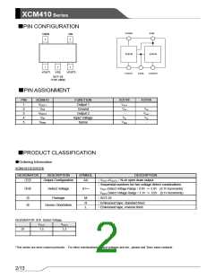
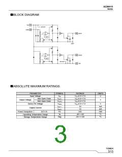
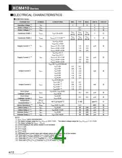
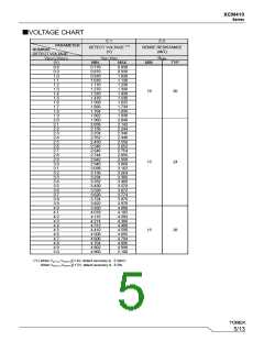
XCM410 Series
■OPERATIONAL EXPLANATION
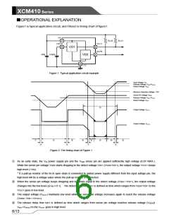
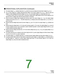
Figure1 is typical application circuit, and Fifure2 is timing chart of figure1.
Figure 1: Typical application circuit example
Input Voltage: VIN
Release Voltage: VDF2+VHYS2
Detect Voltage: VDF2
Minimum Operation Voltage: 1.0V
Sense Pin Voltage: VSEN
Release Voltage: VDF1+VHYS1
Detect Voltage: VDF1
Output Voltage: VOUT1
Output Voltage: VOUT2
Figure 2: The timing chart of Figure 1
①
②
As an early state, the VIN power supply pin and the VSEN sense pin are applied sufficiently high voltage (6.0V MAX.).
While the sense pin voltage VSEN starts dropping to the detect voltage VDF1 (VSEN>VDF1), the output voltage VOUT1 keeps
high level (=VIN).
* If a pull-up resistor of the N-ch open drain is connected to added power supply different from the input voltage pin, the
high level will be a voltage value where the pull-up resistor is connected.
When the sense pin voltage keeps dropping and becomes equal to the detect voltage (VSEN =VDF1), the output voltage
changes into the low level (≦VIN×0.1). The detect delay time tDF1 is defined as time which ranges from VSEN=VDF1 to the
VOUT1 goes in low level.
③
④
The output voltage (VOUT1) maintains low level while the sense pin voltage increases again to reach the release voltage
(VSEN< VDF1 +VHYS1).
The release delay time tDR1 is defined as time which ranges from sense pin voltage reaches release voltage (VSEN
≧
VDF1+VHYS1) to the VOUT1 goes in high level.
6/13

 TOREX [ Torex Semiconductor ]