XCM410 Series
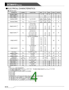
■ELECTRICAL CHARACTERISTICS
●XCM410AA Series
PARAMETER
SYMBOL
CONDITIONS
MIN.
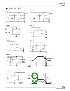
1
TYP.
MAX.
6
UNITS
CIRCUIT
Operating Voltage (*1)
Detect Voltage 1 (*2)
Detect Voltage 2 (*2)
VIN
V
V
V
-
VDF1
VDF2
E-1
E-1
①
②
VDF1
X0.02
VDF2
VDF1
VDF1
X0.08
VDF2
Hysteresis Width 1
Hysteresis Width 2
VHYS1
VHYS2
VIN=1.0~6.0V
V
V
①
②
X0.05
VDF2
VDF2(T)=1.1~5.0V (*3)
X0.02
X0.05
X0.08
VIN=VDF2×0.9
VSEN=VDF1×0.9
VDF2(T)=1.1V~1.9V
VDF2(T)=2.0V~3.9V
VDF2(T)=4.0V~5.0V
VIN=VDF2×1.1
VSEN=VDF1×1.1
VDF2(T)=1.1V~1.9V
VDF2(T)=2.0V~3.9V
VDF2(T)=4.0V~5.0V
SEN=0V VDS=0.5V(N-ch)
VIN=1.0V
Supply Current 1 (*4)
ISS1
1.4
1.5
1.6
3.3
3.5
3.6
μA
μA
③
③
Supply Current 2 (*4)
ISS2
1.8
2.0
3.1
3.6
3.8
4.0
V
0.1
0.8
1.2
1.6
1.8
1.9
0.7
1.6
2.0
2.3
2.4
2.5
VIN=2.0V
Output Current 1
Output Current 2
IOUT1
VIN=3.0V
mA
mA
④
VIN=4.0V
VIN=5.0V
VIN=6.0V
VDS=0.5V(N-ch)
VIN=1.0V (*5)
0.1
0.8
1.2
1.6
0.7
1.6
2.0
2.3
IOUT2
VIN=2.0V (*6)
⑤
VIN=3.0V (*7)
VIN=4.0V (*8)
N-ch Driver
Leakage Current 1
N-ch Driver
VIN=6.0V, VSEN=6.0V,
VOUT=6.0V
ILEAK1
ILEAK2
ΔVDF
0.2
0.2
0.4
0.4
μA
μA
④
④
①
VIN=6.0V
Leakage Current 2
VOUT=6.0V
Temperature
/
-40 oC≦Ta≦85 oC
±100
ppm/oC
Characteristics (*1)
Sense Resistance (*9)
Detect Delay 1 (*10)
Detect Delay 2 (*11)
Release Delay 1 (*12)
Release Delay 2 (*13)
ΔTa・VDF
RSEN
tDF1
VSEN=5.0V VIN=0V
VIN=6.0V
E-2
30
30
30
30
MΩ
μs
μs
μs
μs
⑥
⑦
⑧
⑦
⑧
230
230
200
200
tDF2
VIN=6.0V→1.0V
VIN=6.0V
tDR1
tDR2
VIN=1.0V→6.0V
NOTE:
*1: VOUT1・VOUT2: same characteristics.
*2: The detect voltage range for VDF1 (VOUT1): 0.8V~5.0V. The detect voltage range for VDF2 (VOUT2): 1.1V~5.0V.
*3: The detect voltage for VDF2(T) (VOUT2)
.
*4: Current flowing to the sense resistor is not included.
*5: VDF2(T)>1.0V
*6: VDF2(T)>2.0V
*7: VDF2(T)>3.0V
*8: VDF2(T)>4.0V
*9: Calculated from current value and voltage values at the both ends of the resistor.
*10: Time until VSEN=VDF1 reaches VOUT1=VINx0.1 when VSEN falls.
*11: Time until VIN=VDF2 reaches VOUT2=0.6V when VIN falls.
*12: Time until VSEN=VDF1+VHYS1 reaches VOUT1=VIN when VSEN rises.
*13: Time until VIN=VDF2+VHYS2 reaches VOUT2=5.4V when VIN rises.
4/13

 TOREX [ Torex Semiconductor ]