XC9223/9224 Series
1A Driver Transistor Built-In Step-Down DC/DC Converters
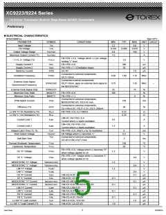
ꢀELECTRICIAL CHARACTERISTICS (Continued)
XC9223B081xx (Continued)
O
Topr=25 C
PARAMETER
SYMBOL
VDF
VDR
VHYS
IDOUT
TDLY
IVDINH
IVDINL
IVDOUTH
IVDOUTL
CONDITIONS
Voltage which VDOUT becomes ”H”D”L”
Voltage which VDOUT becomes ”L”D”H”
VHYS=(VDR-VDF)/VDF x 100
VDIN=VDF x 0.9, apply 0.5V to VDOUT
Time until VDOUT becomes “L” D “H”
VIN=CE=VDIN=6.0V
VIN=CE=6.0V, VDIN=0V
VIN=VDIN=VDOUT=6.0V
VIN=VDIN=6.0V, VDOUT=0V
MIN.
-
-
-
-
-
-
-0.1
-
-1.0
TYP.
0.700
0.745
6
2.5
2
-
-
-
MAX.
-
-
-
-
-
0.1
-
1.0
-
UNIT
V
V
CIRCUIT
Detect Voltage
-
-
-
-
-
-
-
-
-
Release Voltage
Hysteresis Voltage
Output Current
Delay Time
VDIN “H” Current
VDIN “L” Current
VDOUT “H” Current
VDOUT “L” Current
%
mA
ms
µA
µA
µA
µA
-
Test Condition: Unless otherwise stated, VIN=3.6V.
NOTE:
*1: When the difference between the input and the output is small, some cycles may be skipped completely before current maximizes.
If current is further pulled from this state, output voltage will decrease because of P-ch driver ON resistance.
*2: Including hysteresis operating voltage range.
*3: EFFI = { ( output voltage x output current ) / ( input voltage x input current) } x 100
*4: On resistance (Ω)= Lx pin measurement voltage / 100mA
*5: Time until it short-circuits Lx with GND through 1Ω of resistance from a state of operation and is set to Lx=Low from current limit pulse generating.
*6: Integral latch circuit: Latch time may become longer and latch operation may not work when VIN is 3.0V or more.
*7: When temperature is high, a current of approximately 50µA (maximum) may leak.
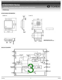
ꢀOPERATIONAL EXPLANATION
Each unit of the XC9223/9224 series consists of a reference voltage source, a ramp wave circuit, error amplifier, PWM comparator, phase compensation
circuit, output voltage adjustment resistors, P-channel MOS driver transistor, N-channel MOS synchronous rectification switching transistor, current limiter
circuit, U.V.L.O. circuit and others. The series compares, using the error amplifier, the internal reference voltage to the CE pin with the voltage fedback from
the VOUT pin via resistors RFB1 and RFB2. Phase compensation is performed on the resulting error amplifier output, to input a signal to the PWM
comparator to determine the turn-on time during PWM operation. The PWM comparator compares, in terms of voltage level, the signal from the error
amplifier with the ramp wave from the ramp wave circuit, and delivers the resulting output to the buffer driver circuit to cause the Lx pin to output a switching
duty cycle. This process is continuously performed to ensure stable output voltage. The current feedback circuit monitors the P-channel MOS driver
transistor current for each switching operation, and modulates the error amplifier output signal to provide multiple feedback signals. This enables a stable
feedback loop even when a low ESR capacitor, such as a ceramic capacitor, is used, ensuring stable output voltage.
<Reference Voltage Source>
The reference voltage source provides the reference voltage to ensure stable output voltage of the DC/DC converter.
<Ramp Wave Circuit>
The ramp wave circuit determines switching frequency. The frequency is fixed internally and can be selected from 1.0MHz and 2.0MHz. Clock pulses
generated in this circuit are used to produce ramp waveforms needed for PWM operation, and to synchronize all the internal circuits.
<Error Amplifier>
The error amplifier is designed to monitor output voltage. The amplifier compares the reference voltage with the feedback voltage divided by the internal
resistors (RFB1 and RFB2). When a voltage lower than the reference voltage is fed back, the output voltage of the error amplifier increases. The gain and
frequency characteristics of the error amplifier output are fixed internally to deliver an optimized signal to the mixer.
Data Sheet
6
DC000019

 TOREX [ Torex Semiconductor ]