XC9223/9224 Series
1A Driver Transistor Built-In Step-Down DC/DC Converters
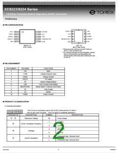
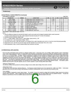
ꢀPIN CONFIGURATION
1 VIN
PGND 10
VIN 1
VDIN 2
AGND 3
VDOUT 4
FB 5
10 PGND
9 LX
2 VDIN
3 AGND
4 VDOUT
5 FB
LX 9
CE 8
8 CE
7 MODE/SYNC
MODE/SYNC 7
6 LIM
LIM 6
MSOP-10
USP-10
(TOP VIEW)
(BOTTOM VIEW)
* Please short the AGND pin and the PGND pin
(pin no. 3 and 10) before use.
* For mounting intensity and heat dissipation, please
refer to recommended mounting pattern and
recommended metal mask when soldering the pad
of USP-10.
ꢀPIN ASSIGNMENT
PIN NUMBER
PIN NAME
VIN
FUNCTIONS
Input
1
2
VDIN
Voltage Detector Input
3
4
AGND
VDOUT
FB
Analog Ground
VD Output
5
Output Voltage Monitor
Over Current Limit Setting
Mode Switch / External Clock Input
Chip Enable
6
LIM
7
MODE/SYNC
CE
8
9
LX
Switch
10
PGND
Power Ground
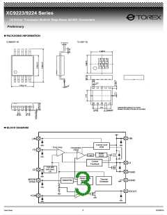
ꢀPRODUCT CLASSIFICATION
ꢁOrdering Information
XC9223B 12345
XC9224B 12345
DESIGNATOR
<The CE pin is commonly used in the DC/DC block and the VD block.>
<No CE pin in the VD block. (The VD block is constantly operated.)>
DESCRIPTION
SYMBOL
DESCRIPTION
1 2
Reference Voltage
08
: Fixed voltage
: 1.0 MHz
1
2
3
4
5
DC/DC Oscillation Frequency
Package
: 2.0 MHz
A
D
R
L
: MSOP-10
: USP-10
: Embossed tape, Standard feed
: Embossed tape, Reverse feed
Device Orientation
Data Sheet
2
DC000019

 TOREX [ Torex Semiconductor ]