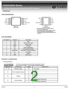
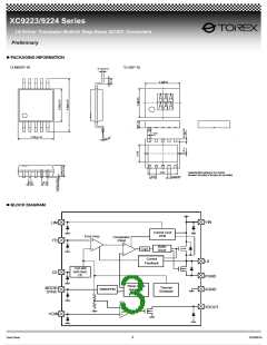
XC9223/9224 Series
1A Driver Transistor Built-In Step-Down DC/DC Converters
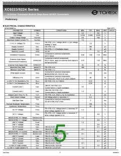
ꢀELECTRICIAL CHARACTERISTICS
XC9223B081xx
O
Topr=25 C
PARAMETER
Input Voltage
FB Voltage
Output Voltage Range
Maximum Output Current (*1)
SYMBOL
VIN
VFB
VOUTSET
IOUTMAX
CONDITIONS
MIN.
2.2
0.784
0.8
TYP.
-
0.800
-
-
MAX.
6.0
0.816
VIN
-
UNIT CIRCUIT
V
V
V
A
-
-
-
-
1.0
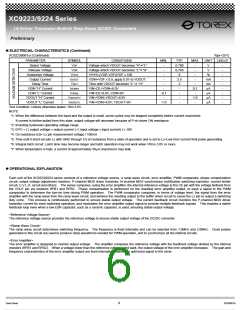
FB=VFB x 0.9, Voltage which Lx pin voltage
holding “L” level
U.V.L.O. Voltage (*2)
VUVLO
-
1.8
-
V
-
Supply Current 1
Supply Current 2
Stand-by Current
IDD1
IDD2
ISTB
FB=VFB x 0.9
FB=VFB x 1.1 (Oscillation stops)
CE=0V
-
-
-
380
30
-
-
-
µA
µA
µA
-
-
-
1.0
Connected to external components,
IOUT=10mA
Oscillation Frequency
FOSC
0.85
1.00
1.15
MHz
-
Connected external components,
IOUT=10mA, apply an external clock signal to
the MODE/SYNC
External Clock Signal
Synchronized Frequency
SYNCOSC
0.75
-
1.25
MHz
--
External Clock Signal Duty
Maximum Duty Ratio
Minimum Duty Ratio
SYNCDTY
MAXDTY
MINDTY
25
100
-
-
-
-
75
-
0
%
%
%
-
-
-
FB=VFB x 0.9
FB=VFB x 1.1
Connected to external components,
MODE/SYNC=0V, IOUT=0.1mA
Connected to external components,
CE=VIN=5.0V, VOUT=3.3V, IOUT=200mA
FB=VFB x 0.9, ILx=100mA
PFM Switch Current
Efficiency (*3)
IPFM
EFFI
-
-
150
94
-
-
mA
%
-
-
Lx SW “H” On Resistance (*4)
Lx SW “L” On Resistance (*4)
RLxH
RLxL
-
-
0.23
0.25
-
-
Ω
Ω
-
-
LIM=0V, FB=VFB x 0.9
Current which Lx starts oscillation
LIM=VIN, FB=VFB x 0.9
Current which Lx starts oscillation
FB=VFB x 0.9, Short Lx by 1Ω resistance
FB Voltage which Lx becomes “L”
Connected to external components,
CE=0VDVIN, IOUT=1mA
Current Limit 1
Current Limit 2
ILIM1
ILIM2
0.5
1.5
-
-
-
-
A
A
-
-
Integral Latch Time (*5, *6)
Short Detect Voltage
TLAT
VSHORT
TSS
-
-
6
0.4
-
-
ms
V
-
-
Soft-Start Time
-
3
-
ms
-
O
Thermal Shutdown Temperature
Hysteresis Temperature
TTSD
THYS
-
-
150
20
-
-
C
-
-
O
C
FB=VFB x 0.9, Voltage which Lx becomes “H”
when voltage applied to CE
FB=VFB x 0.9, Voltage which Lx becomes “L”
when voltage applied to CE
CE “H” Voltage
CE “L” Voltage
VCEH
VCEL
1.2
-
-
-
-
V
V
-
-
0.4
MODE/SYNC “H” Voltage
MODE/SYNC “L” Voltage
LIM “H” Voltage
VMODE/SYNCH
VMODE/SYNCL
VLIMH
1.2
-
-
-
-
-
-
-
-
-
-
-
-
-
-
-
0.4
-
0.4
0.1
-
0.1
-
0.1
-
V
V
V
V
-
-
-
-
-
-
-
-
-
-
-
-
-
-
-
1.2
-
LIM “L” Voltage
CE “H” Current
CE “L” Current
VLIML
ICEH
ICEL
VIN=CE=6.0V
VIN=6.0V, CE=0V
-
µA
µA
µA
µA
µA
µA
µA
µA
µA
µA
-0.1
-
-0.1
-
-0.1
-
-0.1
-
MODE/SYNC “H” Current
MODE/SYNC “L” Current
LIM “H” Current
LIM “L” Current
FB “H” Current
FB “L” Current
Lx SW “H” Leak Current
Lx SW “L” Leak Current (*7)
IMODE/SYNCH
IMODE/SYNCL
ILIMH
VIN=CE=MODE/SYNC=6.0V
VIN=CE=6.0V, MODE/SYNC=0V
VIN=CE=LIM=6.0V
VIN=CE=6.0V, LIM=0V
VIN=CE=FB=6.0V
VIN=CE=6.0V, FB=0V
VIN=LX=6.0V, VCE=0V
VIN=6.0V, LX=CE=0V
ILIML
IFBH
IFBL
ILxH
0.1
-
1.0
-
ILxL
-1.0
Data Sheet
5
DC000019

 TOREX [ Torex Semiconductor ]