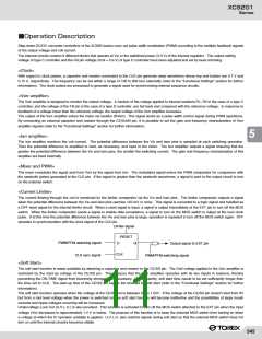
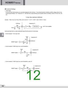
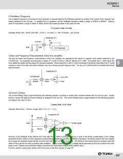
05S_1XC9201/9202新規 02.09.12 15:16 ページ 549
XC9201
Series
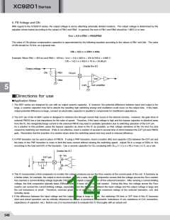
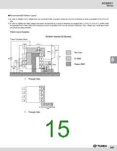
ꢀRecommended Pattern Layout
q In order to stabilize VDD's voltage level, we recommend that a by-pass condenser (CDD) be connected as close as possible to the VIN & VSS
pins.
w In order to stabilize the GND voltage level which can fluctuate as a result of switching, we suggest that C_CLK's, R_CLK's & C_GAIN's GND
be separated from Power GND and connected as close as possible to the VSS pin (by-pass condenser, CDD). Please use a multi layer board
and check the wiring carefully.
Pattern Layout Examples
XC9201 Series (D Series)
2 layer Evaluation Board
L
P-MOS
CDD
CFB
RFB1
VDD Line
1
2
3
4
5
6
7
CL
SD
IC GND
5
RSEN
CIN
Power GND
C_GAIN
RFB2
R_SS
VIN
8
R_CLK
C_SS
C_CLK
Through Hole�
1
2
3
4
5
6
7
8
R_CLK,C_CLK,C_GAIN,RFB2ꢀ�
GND
Through Hole�
549

 TOREX [ Torex Semiconductor ]