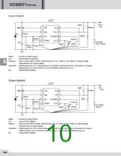
05S_1XC9201/9202新規 02.09.12 15:16 ページ 548
XC9201Series
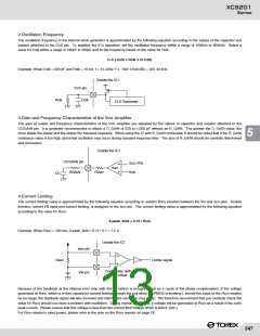
5. FB Voltage and Cfb
With regard to the XC9201D series, the output voltage is set by attaching externally divided resistors. The output voltage is determined by the
equation shown below according to the values of Rfb1 and Rfb2. In general, the sum of Rfb1 and Rfb2 should be 1 MEG Ω or less.
VOUT = 0.9 x (Rfb1 + Rfb2)/Rfb2
The value of Cfb (phase compensation capacitor) is approximated by the following equation according to the values of Rfb1 and fzfb. The value
of fzfb should be 10 kHz, as a general rule.
Cfb = 1/(2 x π x Rfb1 x fzfb)
Example: When Rfb1 = 455 kΩ and Rfb2 = 100 kΩ : VOUT = 0.9 x (455 k + 100 k)/100 k = 4.995 V
: Cfb = 1/(2 x π x 455 k x 10 k) = 34.98 pF.
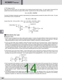
〔Inside the IC〕�
Output voltage
Cfb
Rfb1
FB pin
Verr
Rfb2
0.9V
Verr amplifier
5
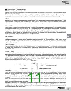
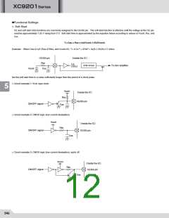
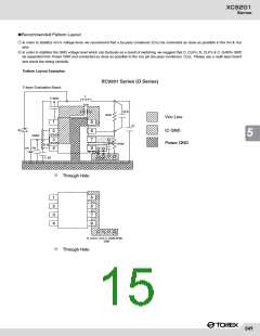
■Directions for use
ꢀApplication Notes
1. The 9201 series are designed for use with an output ceramic capacitor. If, however, the potential difference between input and output is too
large, a ceramic capacitor may fail to absorb the resulting high switching energy and oscillation could occur on the output side. If the input-
output potential difference is large, connect an electrolytic capacitor in parallel to compensate for insufficient capacitance.
2. The EXT pin of the XC9201 series is designed to minimize the through current that occurs in the internal circuitry. However, the gate drive of
external PMOS has a low impedance for the sake of speed. Therefore, if the input voltage is high and the bypass capacitor is attached away
from the IC, the charge/discharge current to the external PMOS may lead to unstable operations due to switching operation of the EXT pin.
As a solution to this problem, place the bypass capacitor as close to the IC as possible, so that voltage variations at the VIN and VSS pins
caused by switching are minimized. If this is not effective, insert a resistor of several to several tens of ohms between the EXT pin and PMOS
gate. Remember that the insertion of a resistor slows down the switching speed and may result in reduced efficiency.
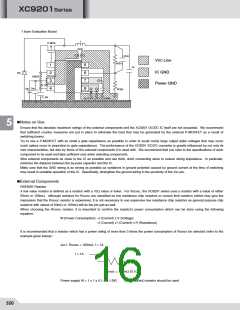
3. A PNP transistor can be used in place of PMOS. If using a PNP transistor, insert a resistor (Rb) and capacitor (Cb) between the EXT pin and
the base of the PNP transistor in order to limit the base current without slowing the switching speed. Adjust Rb in a range of 500Ω to 1kΩ
according to the load and hFE of the transistor. Use a ceramic capacitor for Cb, complying with Cb < 1/ ( 2 x π x Rb x Fosc x 0.7), as a rule.
〔Inside the�IC〕�
VIN
EXT pin
Rb
Cb
4. This IC incorporates a limit comparator to monitor the voltage produces across the RSEN resistor at the current peak of the coil. It functions as
a limiter when, for example, the output is short-circuited. In such a case, the limit comparator senses that the voltage across the RSEN resistor
has reached a current-limiting voltage (typically 150mV) and outputs a signal to turn off the external transistor. After sensing a current-limiting
voltage, the limit comparator typically takes 200nsec before it turns off the external resistor. During this time, the voltage across the RSEN
resistor can exceed the current-limiting voltage, especially when the difference between the input voltage and the output voltage is large and
the coil inductance is small. Therefore, exercise great care in selecting absolute maximum ratings of the external transistor, coil, and
Schottky diode.
5. If the difference between the input voltage and the output voltage is large or small, the switching ON time or OFF time of this IC becomes
short and actual operation can be critically influenced by values of peripheral components 'inductance of coil, resistance of CLK connection,
capacitance of capacitor, etc.) Before use, it is recommended to evaluate this IC thoroughly with an actual unit.
548

 TOREX [ Torex Semiconductor ]