05S_1XC9201/9202新規 02.09.12 15:16 ページ 547
XC9201
Series
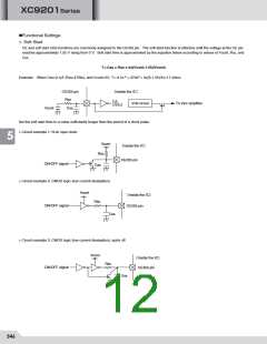
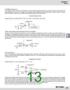
2.Oscillation Frequency
The oscillation frequency of the internal clock generator is approximated by the following equation according to the values of the capacitor and
resistor attached to the CLK pin. To stabilize the IC's operation, set the oscillation frequency within a range of 100kHz to 600kHz. Select a
value for Cclk within a range of 180pF to 300pF and fix the frequency based on the value for Rclk.
f=1/ (-Cclk x Rclk x ln 0.26)
Example: When Cclk = 220 pF and Rclk = 10 kΩ, f = 1/(-220e-12 x 10e3 x ln(0.26)) = 337.43 kHz.
〔Inside the IC〕�
CLK pin
Rclk
Cclk
CLK Generater
3.Gain and Frequency Characteristics of the Verr Amplifier
The gain at output and frequency characteristics of the Verr amplifier are adjusted by the values of capacitor and resistor attached to the
CC/GAIN pin. It is generally recommended to attach a C_GAIN of 220 to 1,000 pF without an R_GAIN. The greater the C_GAIN value, the
more stable the phase and the slower the transient response. When using the IC with R_GAIN connected, it should be noted that if the R_GAIN
resistance value is too high, abnormal oscillation may occur during transient response time. The size of R_GAIN should be carefully determined
and connected.
5
〔Inside the IC〕�
CC/GAIN pin
VOUT/FB
Verr
Vref
RGAIN
RVerr
CC
4.Current Limiting
The current limiting value is approximated by the following equation according to resistor RSEN inserted between the VIN and ISEN pins. Double
function, current FB input and current limiting, is assigned to the ISEN pin. The current limiting value is approximated by the following equation
according to the value for RSEN.
ILpeak_limit = 0.15 / RSEN
Example: When RSEN = 100 mΩ, ILpeak_limit = 0.15 / 0.1 = 1.5 A
〔Inside the IC〕�
Isen pin
Rsen
Limiter signal
Comparator with��
150-mV offset
VIN pin
Because of the feedback at the internal error amp with this IC (which is brought about as a result of the phase compensation of the voltage
generated at RSEN, which is in turn caused by current flowing through the coil when the PMOS is working.), should the value of the RSEN resistor
be too large, the feedback signal will also increase and intermittent oscillation may occur. We therefore recommend that you carefully check the
value for RSEN should you have a problem with oscillation. During normal operations, a voltage will be generated at RSEN as a result of the coil's
peak current. Please ensure that this voltage is less than the current limit voltage which is 90mV (min.).
For RSEN resistor's rated power, please refer to the note on the RSEN resistor on page 18.
547

 TOREX [ Torex Semiconductor ]