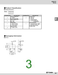
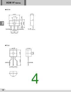
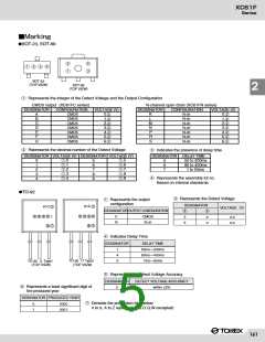
02S_04XC61F 02.09.12 14:04 ページ 163
XC61F
Series
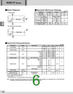
■Functional Description
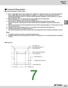
ꢀFunctional Description ( CMOS output )
q
When a voltage higher than the release voltage (VDR) is applied to the voltage input pin (VIN), the voltage will gradually fall.
When a voltage higher than the detect voltage (VDF) is applied to VIN , output (VOUT) will be equal to the input at VIN
.
Note that high impedeance exists at VOUT with the N-channel open drain configuration. If the pin is pulled up, VOUT will be
equal to the pull up voltage.
w
e
When VIN falls below VDF , VOUT will be equal to the ground voltage (VSS) level (detect state).
Note that this also applies to N-channel open drain configurations.
When VIN falls to a level below that of the minimum operating voltage (VMIN ) output will become unstable.
Because the output pin is generally pulled up with N-channel open drain configurations, output will be equal to pull up
voltage.
2
r
When VIN rises above the VSS level (excepting levels lower than minimum operating voltage), VOUT will be equal to VSS until
V
IN reaches the VDR level.
Although VIN will rise to a level higher than VDR, VOUT maintains ground voltage level via the delay circuit.
Following transient delay time, VIN will be output at VOUT
Note that high impedeance exists with the N-channel open drain configuration and that voltage will be dependent on pull up.
t
y
.
Notes :
1. The difference between VDR and VDF represents the hysteresis range.
2. Propagation delay time (tDLY) represents the time it takes for VIN to appear at VOUT once the said voltage has exceeded the
V
DR level.
ꢀTiming Chart
■タイミングチャート�
IN
Input Voltage (V
Detect Release Voltage (VDR
Detect Voltage (VDF
)
)
y
)
Minimum Operating Voltage
(VMIN
)
Ground Voltage (VSS
)
Output Voltage(VOUT
)
Propagation Delay Time (tDLY)
Ground Voltage (VSS
)
w
e
r
q
t
y
163

 TOREX [ Torex Semiconductor ]