02S_04XC61F 02.09.12 14:04 ページ 161
XC61F
Series
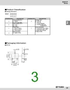
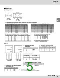
■Marking
ꢀSOT-23, SOT-89
w
r
e
w
q
e r
q
SOT-23
(TOP VIEW)
SOT-89
(TOP VIEW)
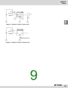
2
q Represents the integer of the Detect Voltage and the Output Configuration
CMOS output (XC61FC series) N-channel open drain (XC61FN series)
DESIGNATOR
CONFIGURATION
CMOS
VOLTAGE (V)
0.w
DESIGNATOR
CONFIGURATION
VOLTAGE (V)
0.w
A
B
C
D
E
F
K
L
N-ch
N-ch
N-ch
N-ch
N-ch
N-ch
N-ch
CMOS
CMOS
CMOS
CMOS
1.w
2.w
3.w
4.w
5.w
6.w
1.w
2.w
3.w
4.w
5.w
6.w
M
N
P
R
S
CMOS
H
CMOS
w Represents the decimal number of the Detect Voltage
e Indicates the presence of delay time
DESIGNATOR VOLTAGE (V) DESIGNATOR VOLTAGE (V)
DESIGNATOR DELAY TIME
q.0
q.1
q.2
q.3
q.4
q.5
q.6
q.7
q.8
q.9
0
1
2
3
4
5
6
7
8
9
5
6
7
50 to 200ms
80 to 400ms
1 to 50ms
r Represents the assembly lot no.
Based on internal standards
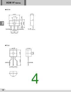
ꢀTO-92
w
Represents the Detect Voltage
w Re
q
Represents the output �
configuration
DESIGNATOR
D
61C
1
5
7
1
L
7
61C
VOLTAGE(V)�
DESIGNATOR OUTPUT CONFIGURATION
w
e
w
3
2
3
4
6
2
3
4
5
6
C
N
CMOS
N-ch
3
5
3
0
3.3
5.0
5
r
Indicates Delay Time
DESIGNATOR
DELAY TIME
1
4
5
50ms~200ms
80ms~400ms
1ms~50ms
TO-92(T Type)�
(TOP VIEW)
TO-92(L Type)�
(TOP VIEW)
t
Represents the Detect Voltage Accuracy
DESIGNATOR
DETECT VOLTAGE ACCURACY
y
Represents a least significant digit of �
the produced yearꢀ�
2
within 2%
DESIGNATOR PRODUCED YEAR
u
Denotes the production lot number�
0 to 9, A to Z repeated(G.I.J.O.Q.W excepted)
0
1
2000
2001
161

 TOREX [ Torex Semiconductor ]