02S_04XC61F 02.09.12 14:04 ページ 162
XC61F Seires
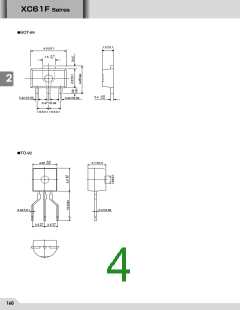
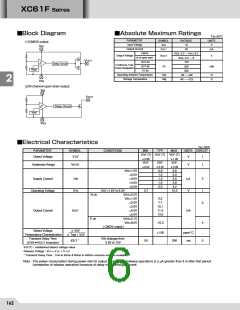
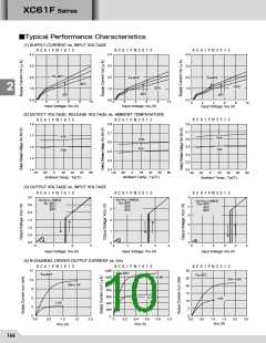
■Block Diagram
■■絶A対b最s大o定lu格t�e Maximum Ratings
Ta=25℃�
PARAMETER
Input Voltage
Output Current
SYMBOL
IN
OUT
RATINGS
UNITS
(1)CMOS output
V
12
50
V
V
IN
I
mA
CMOS
V
SS -0.3 ~ VIN +0.3
Output Voltage
V
OUT
Pd
V
N-ch open drain
SOT-23
V
SS -0.3 ~ 9
150
V
OUT
Delay Circuit
Continuous Total
Power Dissipation
SOT-89
500
mW
Vref
TO-92
300
O
Operating Ambient Temperature
Storage Temperature
Topr
Tstg
-30 ~ +80
C
O
-40 ~ +125
C
2
V
SS
(2)N-channel open drain output
V
IN
VOUT
Delay Circuit
Vref
VSS
■Electrical Characteristics
Ta=25℃�
PARAMETER
SYMBOL
CONDITIONS
MIN
TYP
DF (T)
MAX
UNITS CIRCUIT
VDF (T)
V
VDF (T)
Detect Voltage
V
DF
V
V
1
1
x 0.98
DF
x 0.02
x 1.02
V
VDF
VDF
Hysteresis Range
VHYS
x 0.05
x 0.08
V
IN=1.5V
=2.0V
=3.0V
=4.0V
=5.0V
0.9
1.0
1.3
1.6
2.6
3.0
3.4
3.8
Supply Current
I
SS
µA
2
1
3
2.0
4.2
Operating Voltage
V
IN
V
DF=1.6V to 6.0V
0.7
10.0
V
N-ch
P-ch
VDS=0.5V
V
IN=1.0V
=2.0V
=3.0V
=4.0V
=5.0V
DS=2.1V
2.2
7.7
10.1
11.5
13.0
Output Current
I
OUT
mA
V
VIN=8.0V
-10.0
100
4
( CMOS output )
Detect Voltage
∆ VDF
ppm/°C
-
Temperature Characteristics
Transient Delay Time
∆ Topr
•
VDF
V
IN changes from
0.6V to 10V
ms
tDLY *
50
200
5
(VDR
VOUT inversion)
VDF(T):established detect voltage value
Release Voltage : VDR = V DF + V HYS
* Transient Delay Time : 1ms to 50ms & 80ms to 400ms versions are also available.
Note : The power consumption during power-start to output being stable (release operation) is 2 µA greater than it is after that period�
(completion of release operation) because of delay circuit through current.
162

 TOREX [ Torex Semiconductor ]