ADVANCED INFORMATION
PIN DESCRIPTION
TK654xx
INPUT VOLTAGE PIN (V )
IN
The second function of this pin is to act as a Standby (SB)
input. If this pin is greater than approximately 1.22 V, the
converter will operate normally. Driving this pin low will force
the converter into a "standby" mode where the DC/DC
conversion is disabled. In this "standby" mode, the current
through the inductive element goes to zero; only the filter
capacitor will provide current to the output.
This pin is the positive input supply for the TK654xx. Current
flowing into this pin provides power to the IC and to the
converter output through the inductive element. During the
"on" state, the majority of the current flowing into this pin is
flowingthroughtheinductor.Duringthe"off"and"null"states,
the current into this pin is very small (approximately 18 µA).
The voltage source driving this pin should have relatively low
AC impedance. Good design practices dictate decoupling to
the GND pin.
If neither the Low-Battery or Standby features are needed,
this input pin should be connected directly to the V pin.
IN
Underthismodeofoperation,theTK654xxwillnotturnoff. As
the input voltage approaches the regulation voltages the
TK654xx will act as a P-Channel pass element with
approximately a 2 Ω resistance, going into the linear mode of
operation.
GROUND PIN (GND)
This pin provides the ground connection for the IC.
OUTPUT VOLTAGE PIN (V
)
OUT
LOW BATTERY OUTPUT PIN (LBO)
This pin senses the output voltage of the buck converter.
Input current into this pin is very low (approximately 10 µA).
TheoutputvoltageisresistivelydividedintheICandcompared
to the bandgap voltage. If the output voltage remains greater
than the regulation threshold, the TK654xx remains in a
standby state. As soon as the output voltage drops below the
regulationthreshold,theTK654xxwillinitiatean"on"and"off"
cycle to boost the output voltage.
This pin provides a Low Battery Output (LBO) signal to
indicate when the voltage on the LBI input pin has dropped
below the low battery threshold (1.22 V). This open-drain
output is normally pulled up to either the input supply or the
output supply through a resistive pull-up. The LBO output pin
provides an active-low output. If the LBO is not going to be
used, the pin may be left open.
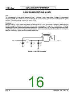
SW PIN
This pin is normally connected to one pin of the inductive
element and an external optional passive schottky rectifier
(optionaltoincreaseefficiency).Theexternalschottkyrectifier
isconnectedbetweenthispinandground.Itisrecommended
that the lead lengths between the rectifier and the pins of the
TK654xx be kept as short as possible to minimize parasitic
inductances.
LOW BATTERY INPUT/STANDBY PIN (LBI/SB)
Thisinputpiniscapableofperformingtwoseparatefunctions
whichwillbedependentupontheapplication'srequirements.
In some applications, this input pin can be used as a Low
Battery Input (LBI). In such an application, this input pin is
typically driven by a resistively divided version of the input
supply (V ). For detailed information on selecting values for
IN
the resistor divider, please refer to Design Considerations on
pages 13 and 14.
Page 12
September 1999 TOKO, Inc.

 TOKO [ TOKO, INC ]