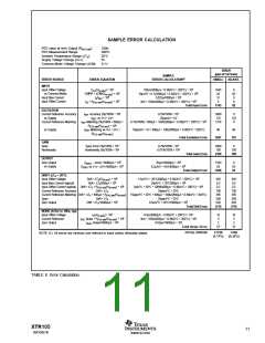
The transfer function through the complete instrumentation
amplifier and voltage-to-current converter is:
APPLICATION INFORMATION
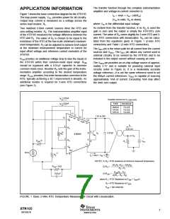
Figure 1 shows the basic connection diagram for the XTR105.
The loop power supply, VPS, provides power for all circuitry.
Output loop current is measured as a voltage across the
series load resistor, RL.
IO = 4mA + VIN • (40/RG)
(VIN in volts, RG in ohms)
where VIN is the differential input voltage.
As evident from the transfer function, if no RG is used the
gain is zero and the output is simply the XTR105’s zero
current. The value of RG varies slightly for 2-wire RTD and 3-
wire RTD connections with linearization. RG can be calcu-
lated from the equations given in Figure 1 (2-wire RTD
connection) and Table I (3-wire RTD connection).
Two matched 0.8mA current sources drive the RTD and
zero-setting resistor, RZ. The instrumentation amplifier input
of the XTR105 measures the voltage difference between the
RTD and RZ. The value of RZ is chosen to be equal to the
resistance of the RTD at the low-scale (minimum) measure-
ment temperature. RZ can be adjusted to achieve 4mA output
at the minimum measurement temperature to correct for
input offset voltage and reference current mismatch of the
XTR105.
The IRET pin is the return path for all current from the current
sources and VREG. The IRET pin allows any current used in
external circuitry to be sensed by the XTR105 and to be
included in the output current without causing an error.
RCM provides an additional voltage drop to bias the inputs of
the XTR105 within their common-mode input range. RCM
should be bypassed with a 0.01µF capacitor to minimize
common-mode noise. Resistor RG sets the gain of the instru-
mentation amplifier according to the desired temperature
range. RLIN1 provides 2nd-order linearization correction to the
RTD, typically achieving a 40:1 improvement in linearity. An
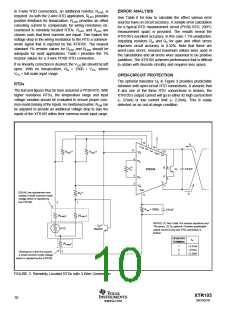
additional resistor is required for 3-wire RTD connections
(see Figure 3).
The VREG pin provides an on-chip voltage source of approxi-
mately 5.1V and is suitable for powering external input
circuitry (refer to Figure 6). It is a moderately accurate
voltage reference—it is not the same reference used to set
the 800µA current references. VREG is capable of sourcing
approximately 1mA of current. Exceeding 1mA may affect
the 4mA zero output.
IR = 0.8mA
IR = 0.8mA
Possible choices for Q1 (see text).
TYPE
PACKAGE
2N4922
TIP29C
TIP31C
TO-225
TO-220
TO-220
12
1
IR1
7.5V to 36V
VLIN
14
13
11
VI+N
IR2
10
V+
VREG
IO
4
RG
4-20 mA
9
8
R(G2)
B
E
0.01µF
Q1
XTR105
VO
+
3
2
RG
VI–N
(3)
RLIN1
RL
VPS
–
IO
7
IRET
RTD
(1)
6
40
RG
RZ
IO = 4mA + VIN • (
)
NOTES: (1) RZ = RTD resistance at minimum measured temperature.
2R1(R2 +RZ) – 4(R2RZ)
RCM = 1kΩ
0.01µF
(2)
(3)
RG
=
R
2 – R1
LIN(R2 – R1)
2(2R1 – R2 – RZ)
R
RLIN1
=
where R1 = RTD Resistance at (TMIN + TMAX)/2
R2 = RTD Resistance at TMAX
RLIN = 1kΩ (Internal)
FIGURE 1. Basic 2-Wire RTD Temperature Measurement Circuit with Linearization.
XTR105
SBOS061B
7
www.ti.com

 TI [ TEXAS INSTRUMENTS ]