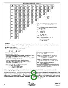
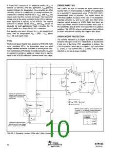
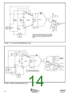
In 3-wire RTD connections, an additional resistor, RLIN2, is
required. As with the 2-wire RTD application, RLIN1 provides
positive feedback for linearization. RLIN2 provides an offset
canceling current to compensate for wiring resistance en-
countered in remotely located RTDs. RLIN1 and RLIN2 are
chosen such that their currents are equal. This makes the
voltage drop in the wiring resistance to the RTD a common-
mode signal that is rejected by the XTR105. The nearest
standard 1% resistor values for RLIN1 and RLIN2 should be
adequate for most applications. Table I provides the 1%
resistor values for a 3-wire Pt100 RTD connection.
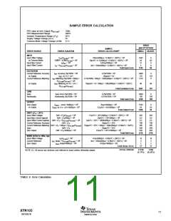
ERROR ANALYSIS
See Table II for how to calculate the effect various error
sources have on circuit accuracy. A sample error calculation
for a typical RTD measurement circuit (Pt100 RTD, 200°C
measurement span) is provided. The results reveal the
XTR105’s excellent accuracy, in this case 1.1% unadjusted.
Adjusting resistors RG and RZ for gain and offset errors
improves circuit accuracy to 0.32%. Note that these are
worst-case errors; ensured maximum values were used in
the calculations and all errors were assumed to be positive
(additive). The XTR105 achieves performance that is difficult
to obtain with discrete circuitry and requires less space.
If no linearity correction is desired, the VLIN pin should be left
open. With no linearization, RG = 2500 • VFS, where
VFS = full-scale input range.
OPEN-CIRCUIT PROTECTION
The optional transistor Q2 in Figure 3 provides predictable
behavior with open-circuit RTD connections. It assures that
if any one of the three RTD connections is broken, the
XTR105’s output current will go to either its high current limit
(≈ 27mA) or low current limit (≈ 2.2mA). This is easily
detected as an out-of-range condition.
RTDs
The text and figures thus far have assumed a Pt100 RTD. With
higher resistance RTDs, the temperature range and input
voltage variation should be evaluated to ensure proper com-
mon-mode biasing of the inputs. As mentioned earlier, RCM can
be adjusted to provide an additional voltage drop to bias the
inputs of the XTR105 within their common-mode input range.
12
IO
1
IR1
VLIN
14
11
IR2
13
VI+N
(1)
(1)
10
V+
RLIN1
RLIN2
VREG
4
RG
R(G1)
9
8
B
E
Q1
0.01µF
XTR105
3
2
RG
VI–N
IO
7
IRET
(1)
EQUAL line resistances here
creates a small common-mode
voltage which is rejected by
the XTR105.
RZ
IO
6
2
1
RCM = 1000Ω
0.01µF
(RLINE2
)
(RLINE1)
NOTES: (1) See Table I for resistor equations and
1% values. (2) Q2 optional. Provides predictable
output current if any one RTD connection is
broken:
(2)
Q2
2N2222
RTD
OPEN RTD
IO
TERMINAL
(RLINE3
)
1
2
3
≈ 2.2mA
≈27mA
≈2.2mA
3
Resistance in this line causes
a small common-mode voltage
which is rejected by the XTR105.
FIGURE 3. Remotely Located RTDs with 3-Wire Connection.
XTR105
10
SBOS061B
www.ti.com

 TI [ TEXAS INSTRUMENTS ]