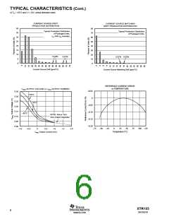
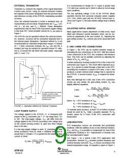
ABSOLUTE MAXIMUM RATINGS(1)
ELECTROSTATIC
DISCHARGE SENSITIVITY
This integrated circuit can be damaged by ESD. Texas Instru-
ments recommends that all integrated circuits be handled with
appropriate precautions. Failure to observe proper handling
and installation procedures can cause damage.
Power Supply, V+ (referenced to the IO pin) ...................................... 40V
Input Voltage, VIN+, VIN– (referenced to the IO pin) .................... 0V to V+
Storage Temperature Range .........................................–55°C to +125°C
Lead Temperature (soldering, 10s)............................................... +300°C
Output Current Limit ................................................................ Continuous
Junction Temperature .................................................................... +165°C
NOTE: (1) Stresses above those listed under “Absolute Maximum Ratings”
may cause permanent damage to the device. Exposure to absolute maximum
conditions for extended periods may affect device reliability.
ESD damage can range from subtle performance degrada-
tion to complete device failure. Precision integrated circuits
may be more susceptible to damage because very small
parametric changes could cause the device not to meet its
published specifications.
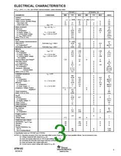
PACKAGE/ORDERING INFORMATION(1)
SPECIFIED
PACKAGE
DESIGNATOR
TEMPERATURE
RANGE
PACKAGE
MARKING
ORDERING
NUMBER
TRANSPORT
MEDIA, QUANTITY
PRODUCT
PACKAGE-LEAD
XTR105
DIP-14
N
"
–40°C to +85°C
XTR105PA
XTR105P
XTR105UA
XTR105UA
XTR105U
XTR105U
XTR105PA
XTR105P
Rails, 25
Rails, 25
"
"
"
XTR105
SO-14 Surface-Mount
D
–40°C to +85°C
XTR105UA
Rails, 58
"
XTR105
"
"
"
D
"
"
XTR105UA/2K5
XTR105U
Tape and Reel, 2500
Rails, 58
SO-14 Surface-Mount
–40°C to +85°C
"
"
XTR105U/2K5
Tape and Reel, 2500
NOTE: (1) For the most current package and ordering information, see the Package Option Addendum located at the end of this data sheet.
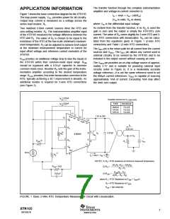
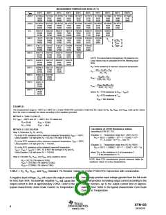
FUNCTIONAL BLOCK DIAGRAM
PIN CONFIGURATION
Top View
DIP and SO
VLIN
IR1
12
IR2
1
14
VREG
V+
800µA
800µA
11
1
2
3
4
5
6
7
IR1
VI–N
RG
RG
NC
IRET
IO
14 IR2
10
13 VI+N
12 VLIN
11 VREG
10 V+
13
4
VI+N
5.1V
B
9
RLIN
1kΩ
Q1
100µA
RG
3
2
E
8
VIN
9
8
B (Base)
E (Emitter)
I = 100µA +
RG
VI–N
975Ω
25Ω
NC = No Internal Connection
7
40
RG
IO = 4mA + VIN
•
(
)
6
IRET
XTR105
2
SBOS061B
www.ti.com

 TI [ TEXAS INSTRUMENTS ]