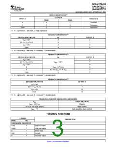
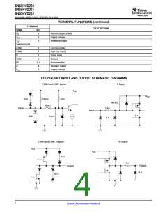
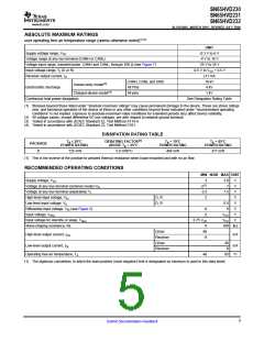
SN65HVD230
SN65HVD231
SN65HVD232
www.ti.com
SLOS346H–MARCH 2001–REVISED JULY 2006
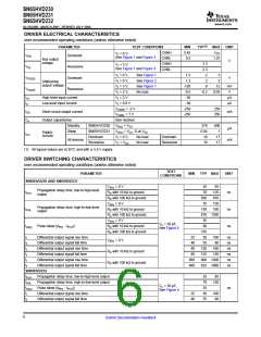
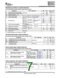
RECEIVER ELECTRICAL CHARACTERISTICS
over recommended operating conditions (unless otherwise noted)
PARAMETER
TEST CONDITIONS
MIN TYP(1)
MAX UNIT
VIT+ Positive-going input threshold voltage
750
900
mV
See Table 1
VIT-
Negative-going input threshold voltage
500
2.4
650
100
mV
Vhys Hysteresis voltage (VIT+ - VIT-
VOH High-level output voltage
VOL Low-level output voltage
)
-6 V ≤ VID ≤ 500 mV, IO = -8 mA, See Figure 5
900 mV ≤ VID ≤ 6 V, IO = 8 mA, See Figure 5
VIH = 7 V
V
0.4
250
350
-30
-20
100
100
µA
µA
VIH = 7 V,
VCC = 0 V
Other input at 0 V,
D = 3 V
II
Bus input current
VIH = -2 V
-200
-100
VIH = -2 V,
Pin-to-ground,
VI = 0.4 sin(4E6πt) + 0.5 V
VCC = 0 V
Ci
CANH, CANL input capacitance
V(D) = 3 V,
V(D) = 3 V,
32
16
pF
pF
Pin-to-pin,
VI = 0.4 sin(4E6πt) + 0.5 V
Cdiff Differential input capacitance
Rdiff Differential input resistance
Pin-to-pin,
V(D) = 3 V
40
20
70
35
100
50
kΩ
kΩ
RI
CANH, CANL input resistance
Supply current
ICC
See driver
(1) All typical values are at 25°C and with a 3.3-V supply.
RECEIVER SWITCHING CHARACTERISTICS
over recommended operating conditions (unless otherwise noted)
PARAMETER
TEST CONDITIONS
MIN TYP MAX UNIT
tPLH
tPHL
tsk(p)
tr
Propagation delay time, low-to-high-level output
Propagation delay time, high-to-low-level output
Pulse skew (|tPHL - tPLH|)
35
35
50
50
10
ns
ns
ns
ns
ns
See Figure 6
Output signal rise time
1.5
1.5
See Figure 6
tf
Output signal fall time
DEVICE SWITCHING CHARACTERISTICS
over recommended operating conditions (unless otherwise noted)
PARAMETER
TEST CONDITIONS
MIN
TYP
MAX UNIT
V(Rs) = 0 V,
See Figure 9
70
105
535
100
155
830
115
Total loop delay, driver input to receiver
output, recessive to dominant
t(LOOP1)
RS with 10 kΩ to ground,
See Figure 9
175
920
135
185
990
ns
ns
RS with 100 kΩ to ground, See Figure 9
V(Rs) = 0 V,
See Figure 9
See Figure 9
Total loop delay, driver input to receiver
output, dominant to recessive
t(LOOP2)
RS with 10 kΩ to ground,
RS with 100 kΩ to ground, See Figure 9
DEVICE CONTROL-PIN CHARACTERISTICS
over recommended operating conditions (unless otherwise noted)
PARAMETER
TEST CONDITIONS
MIN
TYP(1)
MAX
UNIT
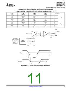
SN65HVD230 wake-up time from standby mode
with RS
0.55
1.5
5
µs
t(WAKE)
See Figure 8
SN65HVD231 wake-up time from sleep mode with
RS
3
µs
(1) All typical values are at 25°C and with a 3.3-V supply.
Submit Documentation Feedback
7

 TI [ TEXAS INSTRUMENTS ]