SN65HVD230
SN65HVD231
SN65HVD232
www.ti.com
SLOS346H–MARCH 2001–REVISED JULY 2006
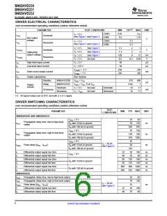
DRIVER ELECTRICAL CHARACTERISTICS
over recommended operating conditions (unless otherwise noted)
PARAMETER
TEST CONDITIONS
MIN
2.45
0.5
TYP(1) MAX
UNIT
CANH
CANL
CANH
CANL
VCC
VI = 0 V,
VOH
Dominant
See Figure 1 and Figure 3
1.25
Bus output
voltage
V
2.3
2.3
2
VI = 3 V,
VOL
Recessive
Dominant
See Figure 1 and Figure 3
VI = 0 V,
See Figure 1
See Figure 2
See Figure 1
No load
1.5
1.2
3
3
VOD(D)
V
VI = 0 V,
2
Differential
output voltage
VI = 3 V,
-120
-0.5
-30
0
12
mV
V
VOD(R)
Recessive
VI = 3 V,
-0.2
0.05
IIH
IIL
High-level input current
Low-level input current
VI = 2 V
µA
µA
VI = 0.8 V
VCANH = -2 V
VCANL = 7 V
See receiver
V(Rs) = VCC
-30
-250
-250
250
250
IOS
Co
Short-circuit output current
mA
Output capacitance
Standby
SN65HVD230
SN65HVD231
Dominant
370
0.04
10
600
1
µA
Sleep
V(Rs) = VCC, D at VCC
Supply
current
ICC
VI = 0 V,
VI = VCC
No load
No load
Dominant
Recessive
17
17
All devices
mA
Recessive
,
10
(1) All typical values are at 25°C and with a 3.3-V supply.
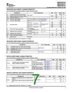
DRIVER SWITCHING CHARACTERISTICS
over recommended operating conditions (unless otherwise noted)
TEST
CONDITIONS
PARAMETER
MIN
TYP MAX
UNIT
SN65HVD230 AND SN65HVD231
V(Rs) = 0 V
35
70
85
125
870
120
180
Propagation delay time, low-to-high-level
output
tPLH
tPHL
tsk(p)
RS with 10 kΩ to ground
ns
ns
ns
RS with 100 kΩ to ground
V(Rs) = 0 V
500
70
Propagation delay time, high-to-low-level
output
RS with 10 kΩ to ground
RS with 100 kΩ to ground
V(Rs) = 0 V
130
870 1200
35
60
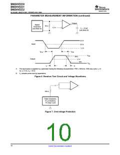
CL = 50 pF,
See Figure 4
Pulse skew (|tPHL - tPLH|)
RS with 10 kΩ to ground
RS with 100 kΩ to ground
370
tr
tf
tr
tf
tr
tf
Differential output signal rise time
Differential output signal fall time
Differential output signal rise time
Differential output signal fall time
Differential output signal rise time
Differential output signal fall time
25
40
50
55
100
80
ns
ns
ns
ns
ns
ns
V(Rs) = 0 V
80
120
125
160
150
RS with 10 kΩ to ground
RS with 100 kΩ to ground
80
600
600
800 1200
825 1000
SN65HVD232
tPLH
tPHL
tsk(p)
tr
Propagation delay time, low-to-high-level output
Propagation delay time, high-to-low-level output
35
70
35
50
55
85
120
CL = 50 pF,
See Figure 4
Pulse skew (|tPHL - tPLH|)
ns
Differential output signal rise time
Differential output signal fall time
25
40
100
80
tf
6
Submit Documentation Feedback

 TI [ TEXAS INSTRUMENTS ]