UCC28740
SLUSBF3A –JULY 2013–REVISED JULY 2013
www.ti.com
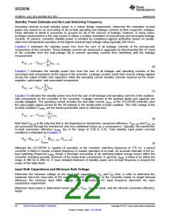
(29)
Feedback Network Biasing
Achieving very low standby power while maintaining high-performance load-step transient response requires
careful design of the feedback network. Optically-coupled secondary-side regulation is used to provide the rapid
response needed when a heavy load step occurs during the no-load condition. One of the most commonly used
devices to drive the optocoupler is the TL431 shunt-regulator, due to its simplicity, regulation performance, and
low cost. This device requires a minimum bias current of 1 mA to maintain regulation accuracy. Together with the
UCC28740 primary-side controller, careful biasing will ensure less than 30 mW of standby power loss at room
temperature. Where a more stringent standby loss limit of less than 10 mW is required, the TLV431 device is
recommended due to its minimum 80-µA bias capability.
Facilitating these low standby-power targets is the approximate 23-µA range of the FB input for full to no-load
voltage regulation. The control-law profile graph (see Figure 15) shows that for FB-input current greater than 22
µA, no further reduction in switching frequency is possible. Therefore, minimum power is converted at fSW(min)
.
However, the typical minimum steady-state operating frequency tends to be in the range of several-hundred
Hertz, and consequently the maximum steady-state FB current at no-load will be less than IFBMAX. Even so,
prudent design practice dictates that IFBMAX should be used for conservative steady-state biasing calculations. At
this current level, VFBMAX can be expected at the FB input.
Referring to the Design Procedure Application Example in Figure 19, the main purpose of RFB4 is to speed up the
turnoff time of the optocoupler in the case of a heavy load-step transient condition. The value of RFB4 is
determined empirically due to the variable nature of the specific optocoupler chosen for the design, but tends to
fall within the range of 10 kΩ to 100 kΩ. A tradeoff must be made between a lower value for faster transient
response and a higher value for lower standby power. RFB4 also serves to set a minimum bias current for the
optocoupler and to drain dark current.
It is important to understand the distinction between steady-state no-load bias currents and voltages which affect
standby power, and the varying extremes of these same currents and voltages which affect regulation during
transient conditions. Design targets for minimum standby loss and maximum transient response often result in
conflicting requirements for component values. Trade-offs, such as for RFB4 as discussed previously, must be
made.
During standby operation, the total auxiliary current (used in Equation 8) is the sum of IWAIT into the IC and the
no-load optocoupler-output current ICENL. This optocoupler current is given by Equation 30.
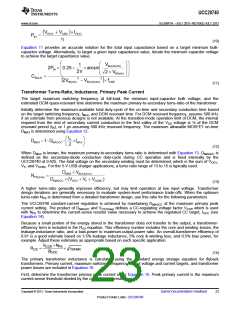
(30)
For fast response, the optocoupler-output transistor is biased to minimize the variation of VCE between full-load
and no-load operation. Connecting the emitter directly to the FB input of the UCC28740 is possible, however, an
unload-step response may unavoidably drive the optocoupler into saturation which will overload the FB input with
full VDD applied. A series-resistor RFB3 is necessary to limit the current into FB and to avoid excess draining of
CVDD during this type of transient situation. The value of RFB3 is chosen to limit the excess IFB and RFB4 current to
an acceptable level when the optocoupler is saturated. Like RFB4, the RFB3 value is also chosen empirically
during prototype evaluation to optimize performance based on the conditions present during that situation. A
starting value may be estimated using Equation 31.
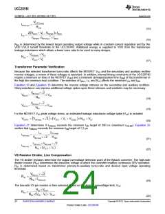
(31)
Note that RFB3 is estimated based on the expected no-load VDD voltage, but full-load VDD voltage will be higher
resulting in initially higher ICE current during the unload-step transient condition. Because RFB3 is interposed
between VE and the FB input, the optocoupler transistor VCE varies considerably more as ICE varies and transient
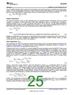
response time is reduced. Capacitor CFB3 across RFB3 helps to improve the transient response again. The value
of CFB3 is estimated initially by equating the RFB3CFB3 time constant to 1 ms, and later is adjusted higher or lower
for optimal performance during prototype evaluation.
26
Submit Documentation Feedback
Copyright © 2013, Texas Instruments Incorporated
Product Folder Links: UCC28740

 TI [ TEXAS INSTRUMENTS ]