UCC28740
SLUSBF3A –JULY 2013–REVISED JULY 2013
www.ti.com
(15)
(16)
NAS is determined by the lowest target operating output voltage while in constant-current regulation and by the
VDD UVLO turnoff threshold of the UCC28740. Additional energy is supplied to VDD from the transformer
leakage-inductance which allows a lower turns ratio to be used in many designs.
(17)
Transformer Parameter Verification
Because the selected transformer turns-ratio affects the MOSFET VDS and the secondary and auxiliary rectifier
reverse voltages, a review of these voltages is important. In addition, internal timing constraints of the UCC28740
require a minimum on time of the MOSFET (tON) and a minimum demagnetization time (tDM) of the transformer in
the high-line minimum-load condition. The selection of fMAX, LP, and RCS affects the minimum tON and tDM
.
Equation 18 and Equation 19 determine the reverse voltage stresses on the secondary and auxiliary rectifiers.
Stray inductance can impress additional voltage spikes upon these stresses and snubbers may be necessary.
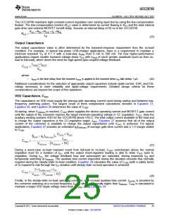
(18)
(19)
For the MOSFET VDS peak voltage stress, an estimated leakage inductance voltage spike (VLK) is included.
(20)
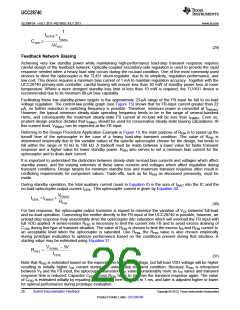
Equation 21 determines if tON(min) exceeds the minimum tON target of 280 ns (maximum tCSLEB). Equation 22
verifies that tDM(min) exceeds the minimum tDM target of 1.2 µs.
(21)
(22)
VS Resistor Divider, Line Compensation
The VS divider resistors determine the output overvoltage detection point of the flyback converter. The high-side
divider resistor (RS1) determines the input-line voltage at which the controller enables continuous DRV operation.
RS1 is determined based on transformer primary-to-auxiliary turns-ratio and desired input voltage operating
threshold.
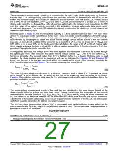
(23)
The low-side VS pin resistor is then selected based on the desired overvoltage limit, VOV
.
(24)
24
Submit Documentation Feedback
Copyright © 2013, Texas Instruments Incorporated
Product Folder Links: UCC28740

 TI [ TEXAS INSTRUMENTS ]