ꢀ
ꢀ
ꢀ
ꢁ
ꢁ
ꢁ
ꢂ
ꢇ
ꢊ
ꢃ
ꢃ
ꢃ
ꢄꢅ
ꢄꢅ
ꢄꢅ
ꢆ
ꢈ
ꢈ
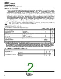
ꢉ ꢀ ꢁꢇ ꢃ ꢄ ꢅ ꢆ
ꢉ ꢀ ꢁ ꢊꢃꢄ ꢅ ꢆ
SLUS329B − JUNE 1998 − REVISED FEBRUARY 2005
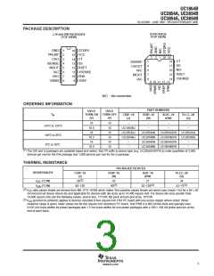
TERMINAL FUNCTIONS
TERMINAL
PACKAGES
J/N/DW Q/L
I/O
DESCRIPTION
NAME
Output of the wide bandwidth current amplifier and one of the inputs to the PWM duty-cycle
comparator. The output signal generated by this amplifier commands the PWM to force the correct
input current. The output can swing from 0.1 V to 7.5 V.
CAO
3
4
O
CT
14
10
18
13
I
I
Capacitor from CT to GND sets the PWM oscillator frequency
A nominal voltage above 2.65 V on this pin allows the device to begin operating. Once operating,
the device shuts off if this pin goes below 2.15 V nominal.
ENA
All bypass and timing capacitors connected to GND should have leads as short and direct as
possible. All voltages are measured with respect GND.
GND
1
2
−
Output of the PWM is a 1.5-A peak totem-pole MOSFET gate driver on GTDRV. This output is
internally clamped to 15 V so that the device can be operated with VCC as high as 35 V. Use a
series gate resistor of at least 5 Ω to prevent interaction between the gate impedance and the
GTDRV output driver that might cause the GTDRV output to overshoot excessively. Some
overshoot of the GTDRV output is always expected when driving a capacitive load.
GTDRV
16
20
O
Current input to the multiplier, proportional to the instantaneous line voltage. This input to the
analog multiplier is a current. The multiplier is tailored for very low distortion from this current input
(IAC) to MOUT, so this is the only multiplier input that should be used for sensing instantaneous
IAC
6
8
I
line voltage. The nominal voltage on IAC is 6 V, so in addition to a resistor from I
to rectified
AC
60 Hz, connect a resistor from IAC to VREF. If the resistor to VREF is one-fourth of the value of the
resistor to the rectifier, then the 6-V offset is cancelled, and the line current has minimal cross-over
distortion.
Switch current sensing input. This is the inverting input to the current amplifier. This input and the
non-inverting input MOUT remain functional down to and below GND. Care should be taken to
avoid taking these inputs below −0.5V, because they are protected with diodes to GND.
ISENSE
MOUT
4
5
5
7
I
Multiplier output and current sense plus. The output of the analog multiplier and the non-inverting
input of the current amplifier are connected together at MOUT. The cautions about taking ISENSE
below −0.5V also apply to MOUT. As the multiplier output is a current, this is a high-impedance
I/O
input similar to I
, so the current amplifier can be configured as a differential amplifier to reject
SENSE
GND noise.
Peak limit. The threshold for PKLMT is 0.0 V. Connect this input to the negative voltage on the
current sense resistor. Use a resistor to REF to offset the negative current sense signal up to GND.
PKLMT
RSET
2
3
I
I
Oscillator charging current and multiplier limit set. A resistor from RSET to ground programs
oscillator charging current. Multiplier output current does not exceed 3.75V divided by the resistor
from RSET to ground.
12
15
Soft-start. SS remains at GND as long as the device is disabled or V
is too low. SS pulls up to
becomes valid and the device is
CC
over 8 V by an internal 14-mA current source when both V
CC
enabled. SS acts as the reference input to the voltage amplifier if SS is below VREF. With a large
capacitor from SS to GND, the reference to the voltage regulating amplifier rises slowly, and
increase the PWM duty cycle slowly. In the event of a disable command or a supply dropout, SS
will quickly discharge to ground and disable the PWM.
SS
13
17
I
VAO
VCC
7
9
I
I
Voltage amplifier output
Positive supply rail
15
19
Used to set the peak limit point and as an internal reference for various device functions. This
voltage must be present for the device to operate.
VREF
9
8
12
10
14
O
I
One of the inputs into the multiplier. This pin provides the input RMS voltage to the multiplier
circuitry.
VRMS
This pin provides the feedback from the output. This input goes into the voltage error amplifier and
the output of the error amplifier is another of the inputs into the multiplier circuit.
VSENSE
11
I
6
www.ti.com

 TI [ TEXAS INSTRUMENTS ]