ꢀ
ꢀ
ꢀ
ꢁ
ꢁ
ꢁ
ꢂ
ꢇ
ꢊ
ꢃ
ꢃ
ꢃ
ꢄꢅ
ꢄꢅ
ꢄꢅ
ꢆ
ꢈ
ꢈ
ꢉ ꢀ ꢁꢇ ꢃ ꢄ ꢅ ꢆ
ꢉ ꢀ ꢁ ꢊꢃꢄ ꢅ ꢆ
SLUS329B − JUNE 1998 − REVISED FEBRUARY 2005
DESCRIPTION (continued)
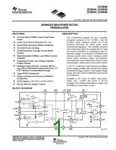
The UC3854A/B products improve upon the UC3854 by offering a wide bandwidth, low offset current amplifier,
a faster responding and improved accuracy enable comparator, a VREF GOOD comparator, UVLO threshold
options (16 V/10 V for offline, 10.5 V/10 V for startup from an auxiliary 12 V regulator), lower startup supply
current, and an enhanced multiply/divide circuit. New features like the amplifier output clamps, improved
amplifier current sinking capability, and low offset VAC pin reduce the external component count while improving
performance. Improved common mode input range of the multiplier output/current amplifier input allow the
designer greater flexibility in choosing a method for current sensing. Unlike its predecessor, R
oscillator charging current and has no effect on clamping the maximum multiplier output current. This current
controls only
SET
is now clamped to a maximum of 2 × I at all times which simplifies the design process and provides foldback
AC
power limiting during brownout and extreme low line conditions.
These devices have limited built-in ESD protection. The leads should be shorted together or the device placed in conductive foam
during storage or handling to prevent electrostatic damage to the MOS gates.
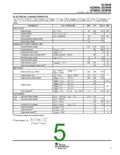
ABSOLUTE MAXIMUM RATINGS
over operating free-air temperature range unless otherwise noted
(1)
UCX854A, UCX854B
UNIT
V
Supply voltage, V
GTDRV current, I
22
CC
Continuous
50% duty cycle
0.5
A
GTDRV
GTDRV Current, I
1.5
A
GTDRV
VSENSE, VRMS ISENSE MOUT
,
11
V
Input voltage
PKLMT
5
10
V
Input current
RSET, IAC, PKLMT, ENA
mA
W
Power dissipation
1
Junction temperature, T
Storage temperature, T
−55 to 150
−65 to 150
300
J
°C
stg
1,6 mm (1/16 inch) from case for 10 seconds
Lead temperature, T
sol,
(1)
Stresses beyond those listed under “absolute maximum ratings” may cause permanent damage to the device. These are stress ratings only,
and functional operation of the device at these or any other conditions beyond those indicated under “recommended operating conditions” is
not implied. Exposure to absolute-maximum-rated conditions for extended periods may affect device reliability. All voltages are with respect to
GND. Currents are positive into and negative out of, the specified terminal. ENA input is internally clamped to approximately 10 V.
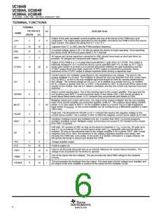
RECOMMENDED OPERATING CONDITIONS
MIN
10
MAX UNIT
Supply voltage, V
CC
20
125
85
V
UC1854X
UC2854X
UC3854X
−55
−40
0
Operating junction temperature, T
°C
J
70
2
www.ti.com

 TI [ TEXAS INSTRUMENTS ]