ꢀ
ꢀ
ꢀ
ꢁ
ꢁ
ꢁ
ꢂ
ꢇ
ꢊ
ꢃ
ꢃ
ꢃ
ꢄ
ꢄ
ꢄ
ꢅ
ꢅ
ꢅ
ꢆ
ꢆ
ꢆ
ꢀꢁꢇ ꢃ ꢄ ꢅ ꢈꢉ
ꢀꢁꢊ ꢃ ꢄ ꢅ ꢈꢉ
SLUS329B − JUNE 1998 − REVISED FEBRUARY 2005
ELECTRICAL CHARACTERISTICS
V
= 18 V, R = 8.2 kΩ, C = 1.5 nF, V
PKLMT
= 1 V, V
= 1.5 V, I
IAC
= 100 µA, I
ISENSE
= 0 V, V
CAO
= 3.5 V, V
VAO
= 5 V, V = 3 V,
VSENSE
CC
T
T
VRMS
−40°C < T < 85°C for the UC2854A and UC2854B, and 0°C < T <70°C for the UC3854A and UC3854B, and T = T (unless otherwise
A
A
A
J
noted)
PARAMETER
TEST CONDITIONS
MIN
TYP
MAX
UNIT
OSCILLATOR
Initial accuracy
T
= 25°C
85
100
1%
115
kHz
A
Voltage stability
Total variation
12 V ≤ V ≤ 18 V
Line, temperature
CC
80
4.9
0.8
120
5.9
1.3
kHz
V
Ramp amplitude (peak-to-peak)
Ramp valley voltage
ENABLE/SOFT-START/CURRENT LIMIT
Enable threshold voltage
Enable hysteresis
2.35
2.55
500
−2
2.80
600
−5
V
V
V
= 2.5 V
mV
µA
ns
FAULT
= 0 V
Enable input bias current
Propagation delay to disable time
Soft-start charge current
Peak limit offset voltage
Peak limit input current
Peak limit propagation delay time
MULTIPLIER
ENA
(1)
Enable overdrive = 100 mV
300
14
V
SS
= 2.5 V
10
−15
24
15
mV
µA
ns
V
= −0.1 V
−200
−100
150
PKLMT
(1)
I
R
= 100 µA,
V
RMS
= 1 V,
AC
Output current, I
AC
limited
−220
−200
−170
= 10 kΩ
SET
µA
µA
Output current, zero
I
= 0 µA,
R
= 10 kΩ
SET
−2.0
−0.2
−200
−22
2.0
AC
Output current, power limited
Output current
V
V
V
V
V
V
= 1.5 V,
= 1.5 V,
= 1.5 V,
= 5 V,
Va = 6 V
Va = 2 V
Va = 5 V
Va = 2 V
Va = 5 V
Va = 6V,
−230
−170
RMS
RMS
RMS
RMS
RMS
RMS
−156
−2
µA
= 5 V,
−14
(2)
Gain constant
= 1.5 V,
T
A
= 25°C
−1.1
12.0
−1.0
−0.9
A/A
GATE DRIVER
V
V
High-level output voltage
Low-level output voltage
I
I
I
I
= −200 mA,
= 200 mA
= 10 mA
V
= 15 V
= 0 V
12.8
1.0
300
0.9
35
OH
OUT
OUT
OUT
OUT
CC
CC
V
2.2
500
1.5
OL
mV
V
Low-level UVLO voltage
= 50 mA,
V
(1)
Output rise time
C
C
C
= 1 nF
= 1 nF
= 10 nF
LOAD
LOAD
LOAD
ns
A
(1)
Output fall time
35
(1)
Output peak current
1.0
(1)
(2)
Ensured by design. Not production tested.
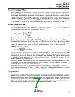
ǒV * 1.5 VNj
IIAC
VAO
Gain constant. (K) +
2
ǒ
Ǔ
ƪV
ƫ
IMOUT
VRMS
5
www.ti.com

 TI [ TEXAS INSTRUMENTS ]