UC1854
UC2854
UC3854
APPLICATIONS INFORMATION (cont.)
PROTECTION INPUTS
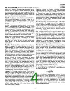
ISENSE/Mult Out (Line current): The voltage drop across
the 0.25 ohm current-sense resistor is applied to pins 4
and 5 as shown. The current-sense amplifier also oper-
ates with high low-frequency gain, but unlike the voltage
amplifier, it is set up to give the current-control loop a very
wide bandwidth. This enables the line current to follow the
line voltage as closely as possible. In the present exam-
ple, this amplifier has a zero at about 500Hz, and a gain
of about 18dB thereafter.
ENA (Enable): The ENA input must reach 2.5 volts be-
fore the REF and GT Drv outputs are enabled. This pro-
vides a means to shut down the gate in case of trouble, or
to add a time delay at power up. A hysteresis gap of
200mV is provided at this terminal to prevent erratic op-
eration. Undervoltage protection is provided directly at pin
15, where the on/off thresholds are 16V and 10V. If the
ENA input is unused, it should be pulled up to VCC
through a current limiting resistor of 100k.
VRMS (RMS line voltage): An important feature of the
UC3854 preregulator is that it can operate with a three-to-
one range of input line voltages, covering everything from
low line in the US (85VAC) to high line in Europe
(255VAC). This is done using line feedforward, which
keeps the input power constant with varying input voltage
(assuming constant load power). To do this, the multiplier
divides the line current by the square of the RMS value of
the line voltage. The voltage applied to pin 8, proportional
to the average of the rectified line voltage (and propor-
tional to the RMS value), is squared in the UC3854, and
then used as a divisor by the multiplier block. The multi-
plier output, at pin 5, is a current that increases with the
current at pin 6 and the voltage at pins 7, and decreases
with the square of the voltage at pin 8.
SS (Soft start): The voltage at pin 13 (SS) can reduce
the reference voltage used by the error amplifier to regu-
late the output DC voltage. With pin 13 open, the refer-
ence voltage is typically 7.5V. An internal current source
delivers approximately -14µA from pin 13. Thus a capaci-
tor connected between that pin and ground will charge
linearly from zero to 7.5V in 0.54C seconds, with C ex-
pressed in microfarads.
PKLIM (Peak current limit): Use pin 2 to establish the
highest value of current to be controlled by the power
MOSFET. With the resistor divider values shown in Figure
1, the 0.0V threshold at pin 2 is reached when the voltage
drop across the 0.25 ohm current sense resistor is
7.5V*2k/10k=1.5V, corresponding to 6A. A bypass capaci-
tor from pin 2 to ground is recommended to filter out very
high frequency noise.
PWM FREQUENCY: The PWM oscillator frequency in
Figure 1 is 100kHz. This value is determined by CT at pin
14 and RSET at pin 12. RSET should be chosen first be-
cause it affects the maximum value of IMULT according to
the equation:
CONTROL INPUTS
VSENSE (Output DC voltage sense): The threshold voltage
for the VSENSE input is 7.5V and the input bias current is
typically 50nA. The values shown in Figure 1 are for an
output voltage of 400V DC. In this circuit, the voltage am-
plifier operates with a constant low frequency gain for
minimum output excursions. The 47nF feedback capacitor
places a 15Hz pole in the voltage loop that prevents
120Hz ripple from propagating to the input current.
−3.75V
RSET
IMULT
=
MAX
This effectively sets a maximum PWM-controlled current.
With RSET=15k,
−3.75V
15k
IMULT
=
= −250µA
MAX
IAC (Line waveform): In order to force the line current
waveshape to follow the line voltage, a sample of the
power line voltage in waveform is introduced at pin 6. This
signal is multiplied by the output of the voltage amplifier in
the internal multiplier to generate a reference signal for
the current control loop.
Also note that the multiplier output current will never ex-
ceed twice IAC.
With the 4k resistor from Mult Out to the 0.25 ohm current
sense resistor, the maximum current in the current sense
resistor will be
This input is not a voltage, but a current (hence IAC). It is
set up by the 220k and 910k resistive divider (see Figure
1). The voltage at pin 6 is internally held at 6V, and the
two resistors are chosen so that the current flowing into
pin 6 varies from zero (at each zero crossing) to about
400µA at the peak of the waveshape. The following for-
mulas were used to calculate these resistors:
−IMULT
×4k
MAX
IMAX
=
= −4A
0.25Ω
Having thus selected RSET, the current sense resistor,
and the resistor from Mult Out to the current sense resis-
tor, calculate CT for the desired PWM oscillator frequency
from the equation
Vpk 260VAC × √2
1.25
CT =
RAC
=
=
= 910k
IACpk
400µA
F × RSET
RAC
4
RREF
=
= 220k
(where Vpk is the peak line voltage)
7

 TI [ TEXAS INSTRUMENTS ]