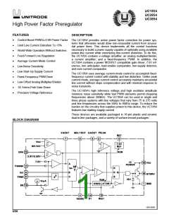
UC1854
UC2854
UC3854
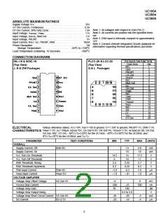
PIN DESCRIPTIONS (cont.)
GT Drv (Pin 16) (gate drive): The output of the PWM is a pedance and the GT Drv output driver that might cause
totem pole MOSFET gate driver on GT Drv. This output is the GT Drv output to overshoot excessively. Some over-
internally clamped to 15V so that the IC can be operated shoot of the GT Drv output is always expected when driv-
with VCC as high as 35V. Use a series gate resistor of at ing a capacitive load.
least 5 ohms to prevent interaction between the gate im-
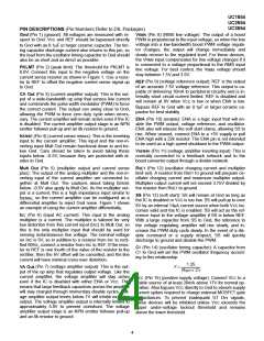
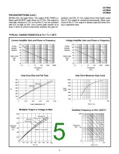
TYPICAL CHARACTERISTICS at TA = TJ = 25°C
Current Amplifier Gain and Phase vs Frequency
Voltage Amplifier Gain and Phase vs Frequency
120
120
Phase
Margin
Phase
Margin
100
100
80
60
40
20
0
80
60
40
20
0
degrees
degrees
Open-Loop
Gain
Open-Loop
Gain
dB
dB
-20
-20
0.1
1
10
100
1000
10000
0.1
1
10
100
1000
10000
Frequency
kHz
Frequency
kHz
Gate Drive Rise and Fall Time
Gate Drive Maximum Duty Cycle
700
600
500
100%
95%
90%
Rise Time
Fall Time
400
ns
Duty
85%
Cycle
300
200
100
0
80%
75%
70%
1
10
100
0
0.01
0.02
0.03
0.04
0.05
R
SET, k Ω
Load Capacitance,
µF
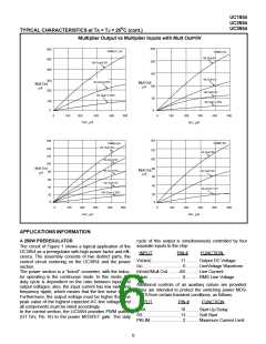
Multiplier Output vs Voltage on Mult
Oscillator Frequency vs RSET and CT
1000
600
500
Mult Out=3V
Mult Out=2V
Mult Out=1
Mult Out=0V
400
100pF
Frequency
Multiplier
Output
µA
kHz
100
200pF
500pF
300
200
VRMS=2V, VA Out=5V
1nF
2nF
100
0
5nF
3nF
10nF
10
10
1
100
0
100 200 300 400 500 600 700
AC, µA
800
I
RSET, k Ω
5

 TI [ TEXAS INSTRUMENTS ]