UC1842/3/4/5
UC2842/3/4/5
UC3842/3/4/5
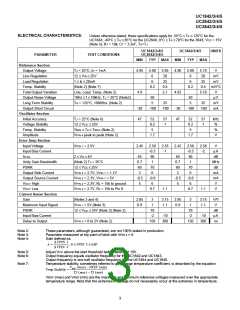
ELECTRICAL CHARACTERISTICS:
Unless otherwise stated, these specifications apply for -55°C ≤ TA ≤ 125°C for the
UC184X; -40°C ≤ TA ≤ 85°C for the UC284X; 0°C ≤ TA ≤ 70°C for the 384X; VCC = 15V
(Note 5); RT = 10k; CT = 3.3nF, TA=TJ.
UC1842/3/4/5
UC2842/3/4/5
UC3842/3/4/5
UNITS
PARAMETER
TEST CONDITIONS
MIN
TYP
MAX
MIN
TYP
MAX
Reference Section
Output Voltage
Line Regulation
Load Regulation
Temp. Stability
Total Output Variation
Output Noise Voltage
Long Term Stability
Output Short Circuit
Oscillator Section
Initial Accuracy
Voltage Stability
Temp. Stability
Amplitude
TJ = 25°C, IO = 1mA
12 ≤ VIN ≤ 25V
4.95
4.9
5.00
6
5.05
20
4.90
4.82
5.00
6
5.10
20
V
mV
mV
1 ≤ I0 ≤ 20mA
6
25
6
25
(Note 2) (Note 7)
0.2
0.4
5.1
0.2
0.4 mV/°C
Line, Load, Temp. (Note 2)
10Hz ≤ f ≤ 10kHz, TJ = 25°C (Note2)
TA = 125°C, 1000Hrs. (Note 2)
5.18
V
50
5
50
5
µV
mV
mA
25
25
-30
47
-100
-180
-30
47
-100
-180
TJ = 25°C (Note 6)
52
0.2
5
57
1
52
0.2
5
57
1
kHz
%
12 ≤ VCC ≤ 25V
TMIN ≤ TA ≤ TMAX (Note 2)
VPIN 4 peak to peak (Note 2)
%
1.7
1.7
V
Error Amp Section
Input Voltage
VPIN 1 = 2.5V
2.45
2.50
-0.3
90
1
2.55
-1
2.42
2.50
-0.3
90
1
2.58
-2
V
µA
dB
MHz
dB
mA
mA
V
Input Bias Current
AVOL
2 ≤ VO ≤ 4V
65
0.7
60
2
65
0.7
60
2
Unity Gain Bandwidth
PSRR
(Note 2) TJ = 25°C
12 ≤ VCC ≤ 25V
70
6
70
6
Output Sink Current
Output Source Current
VOUT High
VPIN 2 = 2.7V, VPIN 1 = 1.1V
VPIN 2 = 2.3V, VPIN 1 = 5V
VPIN 2 = 2.3V, RL = 15k to ground
VPIN 2 = 2.7V, RL = 15k to Pin 8
-0.5
5
-0.8
6
-0.5
5
-0.8
6
VOUT Low
0.7
1.1
0.7
1.1
V
Current Sense Section
Gain
(Notes 3 and 4)
2.85
0.9
3
1
3.15
1.1
2.85
0.9
3
1
3.15
1.1
V/V
V
Maximum Input Signal
PSRR
VPIN 1 = 5V (Note 3)
12 ≤ VCC ≤ 25V (Note 3) (Note 2)
70
-2
70
-2
dB
µA
ns
Input Bias Current
Delay to Output
-10
-10
VPIN 3 = 0 to 2V (Note 2)
150
300
150
300
Note 2:
Note 3:
Note 4:
These parameters, although guaranteed, are not 100% tested in production.
Parameter measured at trip point of latch with VPIN 2 = 0.
Gain defined as
∆ VPIN 1
A =
, 0 ≤ VPIN 3 ≤ 0.8V
∆ VPIN 3
Adjust VCC above the start threshold before setting at 15V.
Note 5:
Note 6:
Output frequency equals oscillator frequency for the UC1842 and UC1843.
Output frequency is one half oscillator frequency for the UC1844 and UC1845.
Temperature stability, sometimes referred to as average temperature coefficient, is described by the equation:
Note 7:
VREF (max) − VREF (min)
Temp Stability =
TJ (max) − TJ (min)
VREF (max) and VREF (min) are the maximum and minimum reference voltages measured over the appropriate
temperature range. Note that the extremes in voltage do not necessarily occur at the extremes in temperature.
3

 TI [ TEXAS INSTRUMENTS ]