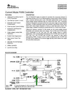
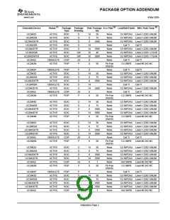
UC1842/3/4/5
UC2842/3/4/5
UC3842/3/4/5
ABSOLUTE MAXIMUM RATINGS(Note 1)
Supply Voltage (Low Impedance Source) . . . . . . . . . . . . . . 30V
Supply Voltage (ICC < 30mA) . . . . . . . . . . . . . . . . . Self Limiting
Output Current. . . . . . . . . . . . . . . . . . . . . . . . . . . . . . . . . . . ±1A
Output Energy (Capacitive Load) . . . . . . . . . . . . . . . . . . . . 5 µJ
Analog Inputs (Pins 2, 3). . . . . . . . . . . . . . . . . . . -0.3V to +6.3V
Error Amp Output Sink Current . . . . . . . . . . . . . . . . . . . . 10 mA
Power Dissipation at TA ≤ 25°C (DIL−8) . . . . . . . . . . . . . . . . . 1 W
Power Dissipation at TA ≤ 25°C (SOIC-14) . . . . . . . . . 725 mW
Storage Temperature Range. . . . . . . . . . . . . . -65°C to +150°C
Junction Temperature Range . . . . . . . . . . . . . -55°C to +150°C
Lead Temperature (soldering, 10 seconds). . . . . . . . . . . 300°C
Note 1:
All voltages are with respect to Pin 5.
All currents are positive into the specified terminal.
Consult Packaging Section of Databook for thermal
limitations and considerations of packages.
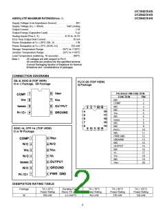
CONNECTION DIAGRAMS
DIL-8, SOIC-8 (TOP VIEW)
N or J Package, D8 Package
PLCC-20 (TOP VIEW)
Q Package
PACKAGE PIN FUNCTION
FUNCTION
PIN
1
N/C
COMP
N/C
2
3
N/C
4
VFB
5
N/C
6
ISENSE
N/C
7
8
N/C
9
SOIC-14, CFP-14. (TOP VIEW)
D or W Package
RT/CT
N/C
10
11
12
13
14
15
16
17
18
19
20
PWR GND
GROUND
N/C
OUTPUT
N/C
VC
VCC
N/C
VREF
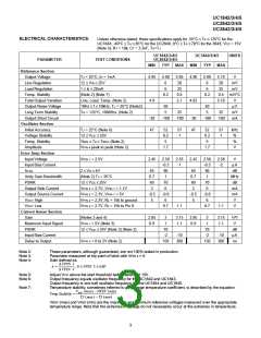
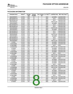
DISSIPATION RATING TABLE
Package
TA ≤ 25°C
Derating Factor
TA ≤ 70°C
TA ≤ 85°C
TA ≤ 125°C
Power Rating
Above TA ≤ 25°C
Power Rating
Power Rating
Power Rating
W
700 mW
5.5 mW/°C
452 mW
370 mW
150 mW
2

 TI [ TEXAS INSTRUMENTS ]