UC17131/2/3
UC27131/2/3
UC37131/2/3
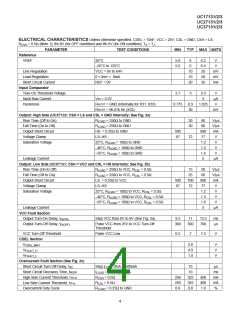
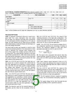
ELECTRICAL CHARACTERISTICS Unless otherwise specified, CDEL = 10nF, VCC = 25V, CSL = GND, CSH = LS;
RCSH = 0.5Ω (Note 1); IN=0V (for OFF condition) and IN=5V (for ON condition); TA = TJ.
PARAMETER TEST CONDITIONS MAX UNITS
MIN
TYP
LED Output
SINK, tDOFF, tROFF
ILEAKAGE
Overall
I
VLED = 7V
5.0
8.0
1
11.0
5
mA
µA
Delay to Output
ICC
3
6
2.8
3
µs
Output Off
2.0
2.3
2.5
mA
mA
mA
IL = 1mA, 250mA (High Side)
IL = 1mA, 250mA (Low Side)
4
Note 1: All test conditions are for a high side configuration as in Fig. 2a, unless otherwise specified.
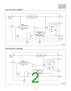
PIN DESCRIPTIONS
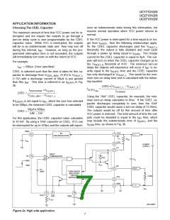
CDEL: A capacitor connected to this pin is used to pro- HS: (For UC37132 and UC37133) The output of the
gram both VCC pulse interruption time and power switching transistor in the high side configuration. The
turn-on delay. The capacitor discharge time corresponds emitter of the output transistor is the HS pin which is con-
to VCC interruption and the charge time to VCC turn-on nected to the load. For the UC37132, the HS pin must be
delay. The ratio between turn-on delay and turn-off delay tied to the CSL pin in a low side application.
will be fixed based on internal charge and discharge cur-
rents and voltage thresholds.
HYST: (For UC37132) The pin used to program the in-
put comparator hysteresis by connecting a resistor to
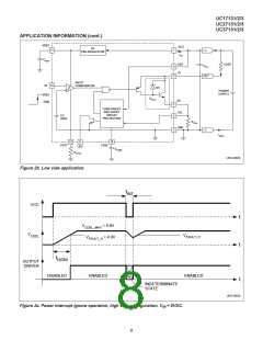
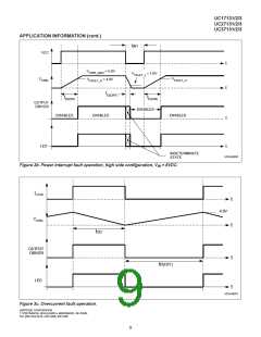
The same fault circuitry and capacitor is used for short
circuit and overload protection. If an overcurrent or short
circuit is detected, the capacitor starts charging and
turns off the output if the condition persists at the end of
its charge time. The output will then operate in a low-duty
cycle mode to protect the IC. After short circuit recovery,
the output will be reactivated in order to check if the short
circuit was removed. If the overcurrent persists the chip
will continue in this pulsing mode.
ground. The hysteresis defaults to 30% with HYST
grounded (internally for UC37131 and UC37133).
3000
VHYST
=
(3330 + RHYST
)
IN: The input to the comparator that detects when the
output transistor should be turned on. The input thresh-
old is 3.0V (1/2 VREF) and the input voltage range is 0V
to VREF.
CSH: (For UC37132 and UC37133) This high side cur-
rent sense pin is used to program the current limit for
high side applications by connecting a resistor between
VCC and CSH. An over load current is detected when
the voltage drop between VCC and CSH exceeds
150mV. For the UC37132, in a high side application, the
CSH pin must be tied to the LS pin; in a low side applica-
tion, the CSH pin must be tied to VCC
LED: Open collector output intended to drive an LED.
This pin is driven low whenever the output is turned off
and is externally pulled high when the output is turned on
(see Fig. 3b and 3c).
LS: (For UC37131 and UC37132) The output of the
switching transistor in the low side configuration. The col-
lector of the output transistor is the LS pin which is con-
nected to the load. For the UC37132, the LS pin must be
tied to the CSH pin in a high side application.
CSL: (For UC37131 and UC37132) This low side cur-
rent sense pin is used to program the current limit for low
side applications by connecting a resistor between CSL
and GND. An over load current is detected when the volt-
age drop between CSL and GND exceeds 150mV. For
the UC37132, in a high side application, the CSL pin
must be tied to GND; in a low side application, the CSL
pin must be tied to the HS pin.
VREF: The 6V regulated reference capable of supplying
up to 8mA. The recommended decoupling capacitor is
1nF.
VCC: The supply voltage for the chip. Decouple this pin
with a good quality ceramic capacitor to ground.
GND: The reference point for the internal reference, all
thresholds, and the return for the remainder of the de-
vice.
5

 TI [ TEXAS INSTRUMENTS ]