UC17131/2/3
UC27131/2/3
UC37131/2/3
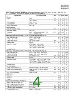
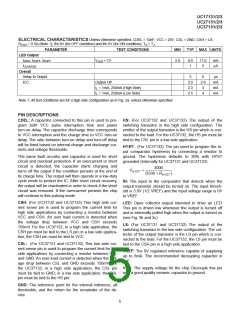
ELECTRICAL CHARACTERISTICS Unless otherwise specified, CDEL = 10nF, VCC = 25V, CSL = GND, CSH = LS;
RCSH = 0.5Ω (Note 1); IN=0V (for OFF condition) and IN=5V (for ON condition); TA = TJ.
PARAMETER TEST CONDITIONS MAX UNITS
MIN
TYP
Reference
VREF
25°C
5.8
5.6
6
6.2
6.4
35
50
35
V
–55°C to 125°C
VCC = 8V to 64V
0 < IREF < 8mA
REF = 0V
6
V
Line Regulation
Load Regulation
10
10
20
mV
mV
mA
Short Circuit Current
Input Comparator
Turn-On Threshold Voltage
Input Bias Current
Hysteresis
2.7
3
3.3
5
V
µA
V
VIN = 3.5V
RHYST = GND (Internally for X31, X33)
RHYST = 96.67k for (X32)
0.775
0.9
30
1.025
mV
Output: High Side (UCX7133: CSH = LS and CSL = GND Internally; See Fig. 2a)
Rise Time (Off to On)
Fall Time (On to Off)
Output Short Circuit
Voltage Clamp
RLOAD = 250Ω to GND
RLOAD = 250Ω to GND
HS = 0.25Ω to GND
30
30
80
80
V/µs
V/µs
mA
V
500
67
900
77
LS–HS
72
Saturation Voltage
25°C, RLOAD = 100Ω to GND
–40°C, RLOAD = 100Ω to GND
–55°C, RLOAD = 100Ω to GND
1.2
1.3
1.4
5
V
V
V
Leakage Current
µA
Output: Low Side (UCX7131; CSH = VCC and CSL = HS Internally; See Fig. 2b)
Rise Time (On to Off)
Fall Time (Off to On)
Output Short Circuit
Voltage Clamp
RLOAD = 250Ω to VCC, RCSL = 0.5Ω
RLOAD = 250Ω to VCC, RCSL = 0.5Ω
LS = 0.25Ω to VCC
15
25
50
60
V/µs
V/µs
mA
V
500
67
700
72
900
77
LS–HS
Saturation Voltage
25°C, RLOAD = 100Ω to VCC, RCSL = 0.5Ω
–40°C, RLOAD = 100Ω to VCC, RCSL = 0.5Ω
–55°C, RLOAD = 100Ω to VCC, RCSL = 0.5Ω
1.2
1.3
1.4
5
V
V
V
Leakage Current
µA
VCC Fault Section
Output Turn-On Delay, tD(ON)
Output Turn-Off Delay, tD(OFF)
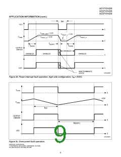
Step VCC from 0V to 8V (See Fig. 3a)
9.5
11
13.5
700
ms
Pulse VCC from 25V to VCC Turn-Off
Threshold
300
500
µs
VCC Turn-Off Threshold
CDEL Section
Pulse VCC Low
6.5
7
7.5
V
VCDEL_MAX
5.8
4.9
1.0
V
V
V
VFAULT_H
VFAULT_L
Overcurrent Fault Section (See Fig. 3c)
Short Circuit Turn-Off Delay, tSC
Short Circuit Recovery Time, tROFF
High Side Current Threshold, ITH-H
Low Side Current Threshold, ITH-L
Overcurrent Duty Cycle
Step ILOAD: 0mA to 400mA
ILOAD = 400mA, 100µs
RCSH = 0.5Ω
75
10
µs
ms
mA
mA
%
250
250
0.6
325
325
0.8
400
400
1.0
RCSL = 0.5Ω
RLOAD = 0.25Ω to GND
4

 TI [ TEXAS INSTRUMENTS ]