UC1517
UC3517
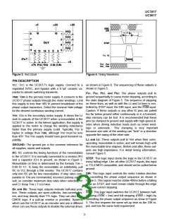
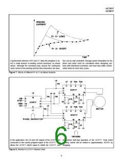
Figure 3. Test Circuit
Figure 4. Timing Waveforms
PIN DESCRIPTION
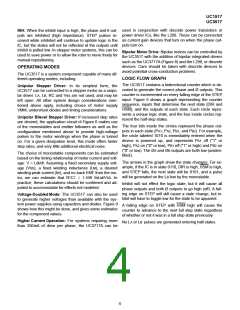
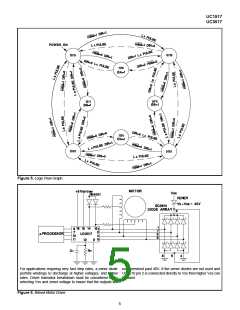
VCC: VCC is the UC3517’s logic supply. Connect to a as shown in Figure 8. The sequencing of these outputs is
shown in Figure 5.
regulated 5VDC, and bypass with a 0.1µF ceramic ca-
pacitor to absorb switching transients.
PA1, PA2, PB1, and PB2: The phase outputs pull to
ground sequentially to cause motor stepping, according to
the state diagram of Figure 5. The sequence of stepping
on these lines, as well as with the LA and LB lines is con-
trolled by STEP input, the DIR input, and the HSM input.
Caution: If these outputs or any other IC pins are pulled
too far below ground either continuously or in a transient,
step memory can be lost. It is recommended that these
pins be clamped to ground and supply with high-speed di-
odes when driving inductive loads such as motor wind-
ings or solenoids. This clamping is very important
because one side of the winding can "kick" in a direction
opposite the swing of the other side.
VMM: VMM is the primary motor supply. It connects to the
UC3517 phase outputs through the motor windings. Limit
this supply to less than 40V to prevent breakdown of the
phase output transistors. Select the nominal VMM voltage
for the desired continuous winding current.
VSS: VSS is the secondary motor supply. It drives the LA
and LB outputs of the UC3517 when a monostable in the
UC3517 is active. In the bilevel application, this supply is
applied to the motor to charge the winding inductance
faster than the primary supply could. Typically, Vss is
higher in voltage than VMM, although VSS must be less
than 40V. The VSS supply should have good transient ca-
pability.
LA and LB: These outputs pull to VSS when their corre-
sponding monostable is active, and will remain high until
the monostable time elapses. Before and after, these out-
puts are high-impedance. For detail timing information,
consult Figure 5.
GROUND: The ground pin is the common reference for
all supplies, inputs and outputs.
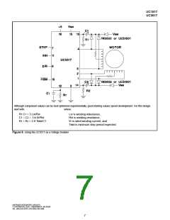
RC: RC controls the timing functions of the monostables
in the UC3517. It is normally connected to a resistor (RT)
and a capacitor (CT) to ground, as shown in Figure 3.
Monostable on time is determined by the formula TON ≈
0.69 RT CT. To keep the monostable on indefinitely, pull
RC to VCC through a 50k resistor. The UC3517 contains
only one RC pin for two monostables. If step rates com-
parable to TON are commanded, incorrect pulsing can re-
sult, so consider maximum step rates when selecting RT
and CT. Keep TON ≤ T STEP MAX.
STEP: This logic input clocks the logic in the UC3517 on
every falling edge. Like all other UC3517 inputs, this input
is TTL/CMOS compatible, and should not be pulled below
ground.
DIR: This logic input controls the motor rotation direction
by controlling the phase output sequence as shown in
Figure 5. This signal must be stable 400ns before a falling
edge on STEP, and must remain stable through the edge
to insure correct stepping.
ØA and ØB: These logic outputs indicate half-step posi-
tion. These outputs are open-collector, low-current driv-
ers, and may directly drive TTL logic. They can also drive
CMOS logic if a pull-up resistor is provided. Systems
which use the UC3517 as an encoder and use a different
driver can use these outputs to disable the external driver,
HSM: This logic input switches the UC3517 between half-
stepping (HSM = low) and full-stepping (HSM = high) by
controlling the phase output sequence as show in Figure
5. This line requires the same set-up time as the DIR in-
put, and has the same hold requirement.
3

 TI [ TEXAS INSTRUMENTS ]