UC1517
UC3517
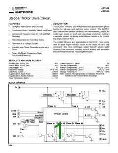
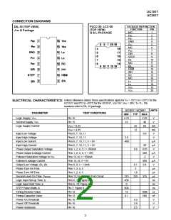
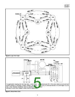
CONNECTION DIAGRAMS
PACKAGE PIN FUNCTION
PLCC-20, LCC-20
(TOP VIEW)
Q & L PACKAGE
DIL-16 (TOP VIEW)
J or N Package
FUNCTION
PIN
N/C
1
PB2
PB1
GND
PA1
N/C
PA2
DIR
STEP
ØB
N/C
ØA
HSM
INH
RC
2
3
4
5
6
7
8
9
10
11
12
13
14
15
16
17
18
19
20
N/C
LA
LB
VSS
VCC
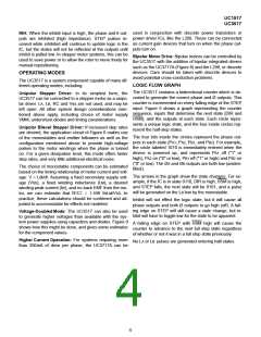
Unless otherwise stated, these specifications apply for TA = -55°C to +125°C for the
ELECTRICAL CHARACTERISTICS:
UC1517 and 0°C to +70°C for the UC3517, Vcc=5V, VSS = 20V, TA=TJ Pin
.
numbers refer to DIL-16 package.
UC1517 / UC3517
UNITS
PARAMETER
TEST CONDITIONS
MIN
4.75
10
TYP
MAX
5.25
40
Logic Supply, VCC
Second Supply, VSS
Logic Supply Current
Pin 16
V
V
Pin 15
VINH = 0.4V
45
12
60
mA
mA
V
VINH = 4.0V
Input Low Voltage
Pins 6, 7, 10, 11
Pins 6, 7, 10, 11
Pins 6, 7, 10, 11; V = 0V
Pins 6, 7, 10, 11; V = 5V
Pins 1, 2, 4, 5; I = 350mA
Pins 1, 2, 4, 5; V = 39V
Pins 13,14; I = 350mA
Pins 13,14; V = 0V
Pins 8, 9; I = 1.6mA
Pins 1, 2, 4, 5
0.8
Input High Voltage
2.0
V
Input Low Current
-400
µA
µA
V
Input High Current
20
0.85
500
-2
Phase Output Saturation Voltage
Phase Output Leakage Current
Follower Saturation Voltage to VSS
Follower Leakage Current
Output Low Voltage, ØA, ØB
Phase Turn-On Time
0.6
µA
V
500
0.4
µA
V
0.1
2
µs
µs
µs
ns
ns
ns
Ω
Phase Turn-Off Time
Pins 1, 2, 4, 5
1.8
325
Second-Level On Time. TMONO
Logic Input Set-up Time, tS
Logic Input Hold Time, th
STEP Pulse Width, tP
Pins 13,14; Figure 3 Test Circuit
Pins 6, 10; Figure 4
Pins 6, 10; Figure 4
Pin 7; Figure 4
Pin 12
275
400
0
375
800
1k
Timing Resistor Value
Timing Capacitor Value
Power-On Threshold
100k
500
Pin 12
0.1
nF
V
Pin 16
4.3
3.8
0.5
Power-Off Threshold
Pin 16
V
Power Hysteresis
Pin 16
V
2

 TI [ TEXAS INSTRUMENTS ]