TUSB1310A
SLLSE32D–NOVEMBER 2010–REVISED MAY 2011
www.ti.com
Contents
1
2
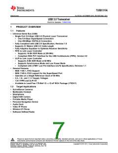
PRODUCT OVERVIEW ......................................................................................................... 7
1.1
1.2
1.3
1.4
Features ...................................................................................................................... 7
Target Applications ......................................................................................................... 7
Introduction .................................................................................................................. 8
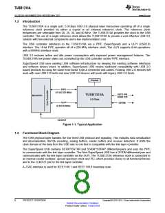
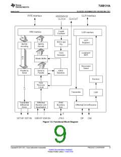
Functional Block Diagram .................................................................................................. 8
PIN DESCRIPTIONS ........................................................................................................... 10
2.1
Configuration Pins ......................................................................................................... 10
2.2
2.3
PIPE ......................................................................................................................... 10
ULPI ......................................................................................................................... 13
2.3.1
ULPI Modes ..................................................................................................... 13
2.4
2.5
2.6
2.7
2.8
2.9
Clocking ..................................................................................................................... 14
JTAG Interface ............................................................................................................. 14
Reset and Output Control Interface ..................................................................................... 14
Strap Options .............................................................................................................. 14
USB Interfaces ............................................................................................................. 15
Special Connect ........................................................................................................... 15
2.10 Power and Ground ........................................................................................................ 16
3
FUNCTIONAL DESCRIPTION ............................................................................................... 18
3.1
Power On and Reset ...................................................................................................... 18
3.1.1
3.1.2
3.1.3
3.1.4
RESETN and PHY_RESETN – Hardware Reset .......................................................... 18
ULPI Reset – Software Reset ................................................................................. 18
OUT_ENABLE - Output Enable .............................................................................. 18
Power Up Sequence ........................................................................................... 18
3.2
Clocks ....................................................................................................................... 19
3.2.1
Clock Distribution ............................................................................................... 19
Output Clock .................................................................................................... 19
3.2.2
3.3
3.4
Power Management ....................................................................................................... 19
USB Power Management ...................................................................................... 20
Receiver Status ............................................................................................................ 21
3.3.1
3.4.1
3.4.2
3.4.3
3.4.4
3.4.5
Clock Tolerance Compensation .............................................................................. 21
Receiver Detection ............................................................................................. 21
8b/10b Decode Errors .......................................................................................... 22
Elastic Buffer Errors ............................................................................................ 22
Disparity Errors ................................................................................................. 22
3.5
3.6
Loopback ................................................................................................................... 22
Adaptive Equalizer ........................................................................................................ 23
4
REGISTERS ...................................................................................................................... 24
4.1
Register Definitions ........................................................................................................ 24
Register Map ............................................................................................................... 24
4.2
4.2.1
4.2.2
4.2.3
4.2.4
4.2.5
4.2.6
Vendor ID and Product ID (00h-03h) ........................................................................ 24
Function Control (04h-06h) .................................................................................... 25
Interface Control (07h-09h) .................................................................................... 26
OTG Control ..................................................................................................... 26
USB Interrupt Enable Rising (0Dh-0Fh) ..................................................................... 26
USB Interrupt Enable Falling (10h-12h) ..................................................................... 27
2
Contents
Copyright © 2010–2011, Texas Instruments Incorporated

 TI [ TEXAS INSTRUMENTS ]