TPS929160-Q1
ZHCSNG0 – APRIL 2023
www.ti.com.cn
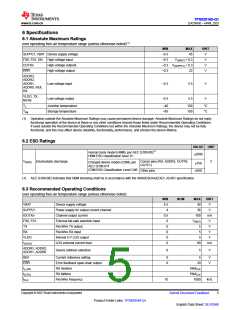
over operating free-air temperature range (unless otherwise noted)
MIN
45
NOM
MAX
UNIT
%
DSYNC
TA
Synchronization pulse dutycycle
Ambient temperature
50
55
125
150
–40
–40
°C
TJ
Junction temperature
°C
6.4 Thermal Information
TPS929160-Q1
THERMAL METRIC(1)
HTSSOP (DCP)
UNIT
38 PINS
27.7
16.6
8.4
RθJA
Junction-to-ambient thermal resistance
Junction-to-case (top) thermal resistance
Junction-to-board thermal resistance
°C/W
°C/W
°C/W
°C/W
°C/W
°C/W
RθJC(top)
RθJB
ΨJT
Junction-to-top characterization parameter
Junction-to-board characterization parameter
Junction-to-case (bottom) thermal resistance
0.3
ΨJB
8.3
RθJC(bot)
1.3
(1) For more information about traditional and new thermal metrics, see the Semiconductor and IC Package Thermal Metrics application
report.
6.5 Electrical Characteristics
TJ = –40°C to 150°C, V(VBAT) = 4.5-40 V, V(SUPPLY) = 4-36 V, for digital outputs, C(LOAD) = 20 pF, (unless otherwise noted).
PARAMETER
TEST CONDITIONS
MIN
TYP
MAX UNIT
BIAS
V(VBAT)
ISD(VBAT)
Operating input voltage
4.5
12
5
40
10
V
Shutdown current, VBAT pin
V(VBAT) = 12 V, EN = L
µA
Quiescent current, all-channels-off,
VBAT pin
V(VBAT) = 12 V, EN = H, R(REF) = 8.45
kΩ, REFRANGE = 11b, all-output OFF
1.6
2.8
2.0
4.0
mA
mA
IQ(VBAT)
V(VBAT) = 12 V, EN = H, R(REF) = 8.45
kΩ, REFRANGE = 11b, PWMOUTXn
= 0, all-output ON
Quiescent current, all-channels-on,
VBAT pin
V(VBAT) = 12 V, V(SUPPLY) = 12 V, EN
= H, R(REF) = 8.45 kΩ, REFRANGE =
11b, all-output OFF
Quiescent current, all-channels-off,
SUPPLY pin
4.9
5.2
10
µA
IQ(SUPPLY)
V(VBAT) = 12 V, V(SUPPLY) = 12 V, EN
= H, R(REF) = 8.45 kΩ, REFRANGE =
11b, PWMOUTXn = 0, all-output ON
Quiescent current, all-channels-on,
SUPPLY pin
8.0
mA
Quiescent current, fail-safe state fault V(VBAT) = 12 V, V(SUPPLY) = 12 V, fail-
mode, VBAT pin safe state, all-output OFF, ERR = LOW
IFAULT(VBAT)
1.3
5
2.0
10
mA
µA
Quiescent current, fail-safe state fault V(VBAT) = 12 V, V(SUPPLY) = 12 V, fail-
IFAULT(SUPPLY)
mode, SUPPLY pin
safe state, all-output OFF, ERR = LOW
ILKG(SUPPLY)
V(POR_rising)
V(POR_falling)
V(LDO)
Supply leakage current
V(SUPPLY) = 36 V, EN = L
0.08
4.2
4
5
4.4
µA
V
Power-on-reset rising threshold
Power-on-reset falling threshold
LDO output voltage
4
3.8
4.2
V
V(VBAT) > 5.6 V, I(LDO) = 80 mA
4.75
5
5.25
80
V
I(LDO)
LDO output current capability
LDO output current limit
mA
mA
V
I(LDO_LIMIT)
V(LDO_DROP)
V(LDO_DROP)
V(LDO_POR_rising)
V(LDO_POR_falling)
110
LDO maximum dropout voltage
LDO maximum dropout voltage
LDO power-on-reset rising threshold
LDO power-on-reset falling threshold
I(LDO) = 80 mA
I(LDO) = 50 mA
0.5
0.3
0.9
0.6
3.25
3
V
2.75
2.5
3.00
2.75
V
V
Copyright © 2023 Texas Instruments Incorporated
English Data Sheet: SLVSG60
6
Submit Document Feedback
Product Folder Links: TPS929160-Q1

 TI [ TEXAS INSTRUMENTS ]