TPS7H5005-SEP, TPS7H5006-SEP, TPS7H5007-SEP, TPS7H5008-SEP
www.ti.com
SLVSGG1 – FEBRUARY 2022
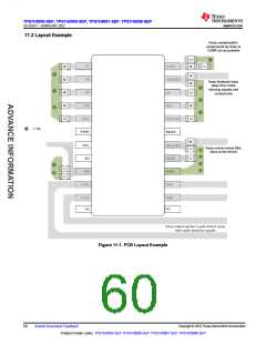
11 Layout
11.1 Layout Guidelines
In order to increase the reliability of the converter design using the TPS7H500x-SEP, the following layout
guidelines should be followed.
•
Route the feedback trace as far away as possible from power magnetics components (inductor and/or power
transformer) and other noise inducting traces on the printed circuit board (PCB) such as the switch node. If
the feedback trace is routed beneath the power magnetic component, ensure that this trace is on another
layer of the PCB with at least one ground layer separating the trace from the inductor or transformer.
Minimize the copper area of the converter switch node for the best noise performance and reduction of
parasitic capacitance to reduce switching losses. Ensure that any noise sensitive signals, such as the
feedback trace, are routed away from this node as it contains a high dv/dt switching signal.
All high di/dt and dv/dt switching loops in the power stage should have the paths minimized. This will help to
reduce EMI, lower stresses on the power devices, and reduce any noise coupling into the control loop.
Keep the analog ground of the controller (AVSS) separate from the power ground of the power stage that
contains high frequency, high di/dt currents. These two grounds should be connected at a single point in the
PCB layout. The sources of power semiconductor switches, the returns for bulk input capacitors of the power
stage, and the ouput capacitor return should all be connected to the PCB power ground.
All high current traces on the PCB should be short, direct, and as wide as possible. A good rule is to make
the traces a minimum of 15 mils (0.381 mm) per ampere.
•
•
•
•
•
Place all filtering and bypass capacitors for VIN, REFCAP, and VLDO as close as possible to the controller.
Surface mount ceramic capacitors with lower ESR and ESL are recommended as these reduce the potential
for noise coupling compared to through-hole capacitors. Care should be taken to minimize the loop area
formed by the bypass capacitor connection, the respective pin, and AVSS. Each bypass capacitor should
have a good, low impedance connection to AVSS.
•
•
•
External compensation components should be placed near the COMP pin of the controller. Surface mount
components are recommended here as well.
Attempt to keep the resistor divider used to generate the voltage at VSENSE close to the device in order to
reduce noise coupling. Minimize stray capacitance to the VSENSE pin.
OUTA, OUTB, SRA, and SRB are used to drive the inputs of a gate driver, isolator, or gate drive transformer.
The PCB traces connected to these pins carry high dv/dt signals. Reduce noise coupling by routing these
these PCB traces away from any traces connected to VSENSE, COMP, RT, CS_ILIM, HICC, LEB, RSC, PS,
and SP.
•
•
In addition to utilizing the leading edge blank time programmability of the controller, RC filtering may be
required for the sensed current signal input to CS_ILIM. Keep the resistor and capacitor in close vicinity to
CS_LIM to filter any ringing and/or spikes that may be present on the sensed current signal.
When operating in internal oscillator mode with SYNC as an output, route the SYNC signal away from
noise sensitive signals/pins such as VSENSE, COMP, RT, CS_ILIM, LEB, RSC, PS, and SP. Special care
should be taken to eliminate noise from SYNC to HICC since these pins are adjacent to one another. It is
recommended that the capacitor from HICC to AVSS be at least 3.3 nF to help with the reduction of the
noise.
Copyright © 2022 Texas Instruments Incorporated
Submit Document Feedback
59
Product Folder Links: TPS7H5005-SEP TPS7H5006-SEP TPS7H5007-SEP TPS7H5008-SEP

 TI [ TEXAS INSTRUMENTS ]