TPS7A80xx
SBVS135A –JUNE 2010–REVISED JUNE 2010
www.ti.com
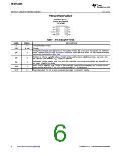
PIN CONFIGURATION
DRB PACKAGE
3mm x 3mm SON-8
(TOP VIEW)
OUT
OUT
1
2
3
4
8
7
6
5
IN
IN
FB/SNS
GND
NR
EN
Table 1. PIN DESCRIPTIONS
NAME
IN
PIN NO.
7, 8
DESCRIPTION
Unregulated input supply.
Ground.
GND
4, pad
Driving the enable pin (EN) high turns on the regulator. Driving this pin low puts the regulator into shutdown
mode. Refer to Shutdown in the Application Information section for more details. EN must not be left floating
and can be connected to IN if not used.
EN
5
Connect an external capacitor between this pin and ground to reduce output noise to very low levels. Also,
the capacitor slows down the VOUT ramp (RC softstart).
NR
FB
6
3
Adjustable voltage version only. This pin is the input to the control loop error amplifier and is used to set
the output voltage of the device.
Fixed voltage versions only. This pin is the input to the control loop error amplifier and is used to set the
output voltage of the device. This pin is to be shorted to OUT at load devices.
SNS
OUT
3
1, 2
Regulator output. A 4.7mF or larger capacitor of any type is required for stability.
6
Submit Documentation Feedback
Copyright © 2010, Texas Instruments Incorporated

 TI [ TEXAS INSTRUMENTS ]