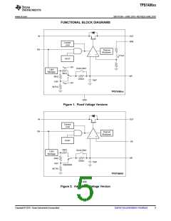
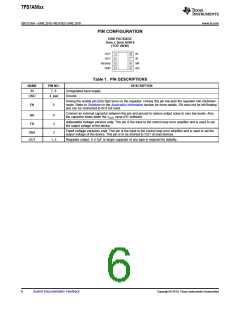
TPS7A80xx
SBVS135A –JUNE 2010–REVISED JUNE 2010
www.ti.com
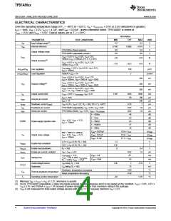
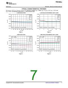
ELECTRICAL CHARACTERISTICS
Over the operating temperature range of TJ = –40°C to +125°C, VIN = VOUT(TYP) + 0.5V or 2.2V (whichever is greater),
IOUT = 1mA, VEN = 2.2V, COUT = 4.7mF, and CNR = 0.01mF, unless otherwise noted. TPS7A8001 is tested at
VOUT = 0.8V and VOUT = 6.0V. Typical values are at TJ = +25°C.
TPS7A80xx
PARAMETER
Input voltage range(1)
TEST CONDITIONS
MIN
2.2
TYP
MAX
6.5
UNIT
VIN
V
V
V
V
VNR
Internal reference
0.790
0.8
0.800
0.810
5.0
TPS7A80xx (fixed versions)
Output voltage range
Output accuracy(2)
TPS7A8001 (adjustable version)
0.8
6.0
VOUT + 0.5V ≤ VIN ≤ 6.0V, VIN ≥ 2.5V,
100mA ≤ IOUT ≤ 500mA, 0°C ≤ TJ ≤ 85°C
VOUT
-2.0
+2.0
+3.0
%
%
VOUT + 0.5V ≤ VIN ≤ 6.5V, VIN ≥ 2.2V,
100mA ≤ IOUT ≤ 1A
–3.0
±0.3
VOUT(NOM) + 0.5V ≤ VIN ≤ 6.5V, VIN ≥ 2.2V,
IOUT = 100mA
ΔVOUT/ΔVIN
ΔVOUT/ΔIOUT
Line regulation
Load regulation
150
2
mV/V
mV/mA
mV
100mA ≤ IOUT ≤ 1A
VOUT + 0.5V ≤ VIN ≤ 6.5V, VIN ≥ 2.2V,
IOUT = 500mA, VFB = GND or VSNS = GND
250
350
500
VOUT + 0.5V ≤ VIN ≤ 6.5V, VIN ≥ 2.5V,
IOUT = 750mA, VFB = GND or VSNS = GND
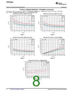
VDO
Dropout voltage(3)
mV
mV
VOUT + 0.5V ≤ VIN ≤ 6.5V, VIN ≥ 2.5V,
IOUT = 1A, VFB = GND or VSNS = GND
ICL
Output current limit
Ground pin current
VOUT = 0.85 × VOUT(NOM), VIN ≥ 3.3V
1100
1400
60
2000
100
350
2
mA
mA
IOUT = 1mA
IGND
IOUT = 1A
mA
ISHDN
IFB
Shutdown current (IGND
Feedback pin current
Sense pin current
)
VEN ≤ 0.4V, VIN ≥ 2.2V, RL = 1kΩ, 0°C ≤ TJ ≤ 85°C
TPS7A8001 (adjustable), VIN = 6.5V, VFB = 0.8V
TPS7A80xx (fixed), VIN = 6.5V, VSNS = VOUT(NOM)
f = 100Hz
0.20
mA
0.02
1.0
1.0
mA
ISNS
0.02
mA
48
dB
f = 1kHz
63
63
dB
VIN = 4.3V, VOUT = 3.3V,
IOUT = 750mA
PSRR
Power-supply rejection ratio
f = 10kHz
dB
f = 100kHz
f = 1MHz
57
dB
38
dB
CNR = 0.001mF
15.6 × VOUT
15.6 × VOUT
15.1 × VOUT
mVRMS
mVRMS
mVRMS
V
BW = 100Hz to 100kHz,
VIN = 4.3V, VOUT = 3.3V,
IOUT = 100mA
VN
Output noise voltage
Enable high (enabled)
CNR = 0.01mF
CNR = 0.1mF
2.2V ≤ VIN ≤ 3.6V, RL = 1kΩ
3.6V < VIN ≤ 6.5V, RL = 1kΩ
RL = 1kΩ
1.2
1.35
0
VEN(HI)
V
VEN(LO)
IEN(HI)
Enable low (shutdown)
0.4
1.0
V
Enable pin current, enabled
VIN = VEN = 6.5V
0.02
0.1
mA
VOUT(NOM) = 3.3V,
CNR = 1nF
ms
tSTR
Startup time
VOUT = 0% to 90% VOUT(NOM)
RL = 3.3kΩ, COUT = 4.7mF
,
CNR = 10nF
1.6
ms
Undervoltage lockout
Hysteresis
VIN rising, RL = 1kΩ
VIN falling, RL = 1kΩ
1.86
–40
2
75
2.10
V
UVLO
mV
°C
°C
°C
Shutdown, temperature increasing
Reset, temperature decreasing
+160
+140
TSD
TJ
Thermal shutdown temperature
Operating junction temperature
+125
(1) Minimum VIN = VOUT + VDO or 2.2V, whichever is greater.
(2) As for TPS7A8001 (adjustable); it does not include external resistor tolerances and it is not tested at this condition: VOUT = 0.8V, 4.5V ≤
IN ≤ 6.5V, and 750mA ≤ IOUT ≤ 1A because of power dissipation higher than maximum rating of the package.
(3) VDO is not measured for fixed output voltage devices with VOUT < 1.7V because minimum VIN = 2.2V.
V
4
Submit Documentation Feedback
Copyright © 2010, Texas Instruments Incorporated

 TI [ TEXAS INSTRUMENTS ]