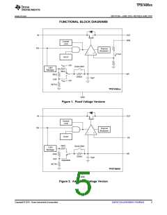
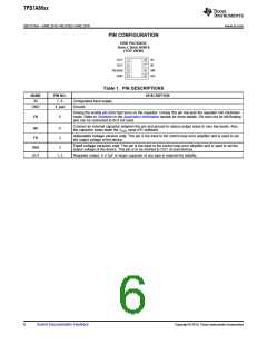
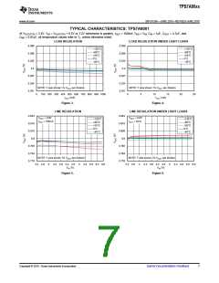
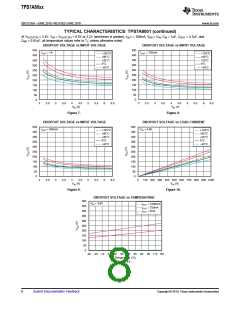
TPS7A80xx
SBVS135A –JUNE 2010–REVISED JUNE 2010
www.ti.com
This integrated circuit can be damaged by ESD. Texas Instruments recommends that all integrated circuits be handled with
appropriate precautions. Failure to observe proper handling and installation procedures can cause damage.
ESD damage can range from subtle performance degradation to complete device failure. Precision integrated circuits may be more
susceptible to damage because very small parametric changes could cause the device not to meet its published specifications.
ORDERING INFORMATION(1)
(2)
PRODUCT
VOUT
TPS7A80xxyyyz
XX is nominal output voltage (for example, 28 = 2.8V, 285 = 2.85V, 01 = Adjustable).
YYY is package designator.
Z is package quantity.
(1) For the most current package and ordering information see the Package Option Addendum at the end of this document, or visit the
device product folder on www.ti.com.
(2) Output voltages from 0.9V to 5.0V in 50mV increments are available through the use of innovative factory EEPROM programming;
minimum order quantities may apply. Contact factory for details and availability.
ABSOLUTE MAXIMUM RATINGS
over operating free-air temperature range (unless otherwise noted)(1)
VALUE
MIN
–0.3
–0.3
MAX
+7.0
+3.6
UNIT
V
IN
FB, NR
V
Voltage
VIN
+
EN
–0.3
V
0.3(2)
+7.0
OUT
–0.3
V
A
Current
OUT
Internally Limited
Operating virtual junction, TJ
–55
–55
+150
°C
°C
kV
Temperature
Storage, Tstg
+150
2
Human body model (HBM) QSS 009-105 (JESD22-A114A)
Electrostatic Discharge Rating(3)
Charged device model (CDM) QSS 009-147
(JESD22-C101B.01)
500
V
(1) Stresses beyond those listed under Absolute Maximum Ratings may cause permanent damage to the device. These are stress ratings
only, and functional operation of the device at these or any other conditions beyond those indicated is not implied. Exposure to
absolute-maximum-rated conditions for extended periods my affect device reliability.
(2) VEN absolute maximum rating is VIN + 0.3V or +7.0V, whichever is smaller.
(3) ESD testing is performed according to the respective JESD22 JEDEC standard.
2
Submit Documentation Feedback
Copyright © 2010, Texas Instruments Incorporated

 TI [ TEXAS INSTRUMENTS ]