TPS736xx
www.ti.com
SBVS038K–SEPTEMBER 2003–REVISED SEPTEMBER 2005
Reverse Current
expected ambient temperature and worst-case load.
The NMOS pass element of the TPS736xx provides
inherent protection against current flow from the
output of the regulator to the input when the gate of
the pass device is pulled low. To ensure that all
charge is removed from the gate of the pass element,
the enable pin must be driven low before the input
voltage is removed. If this is not done, the pass
element may be left on due to stored charge on the
gate.
The internal protection circuitry of the TPS736xx has
been designed to protect against overload conditions.
It was not intended to replace proper heat sinking.
Continuously running the TPS736xx into thermal
shutdown will degrade reliability.
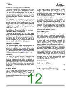
Power Dissipation
The ability to remove heat from the die is different for
each package type, presenting different consider-
ations in the PCB layout. The PCB area around the
device that is free of other components moves the
heat from the device to the ambient air. Performance
data for JEDEC low and high K boards are shown in
the Power Dissipation Ratings table. Using heavier
copper will increase the effectiveness in removing
heat from the device. The addition of plated
through-holes to heat-dissipating layers will also im-
prove the heat-sink effectiveness.
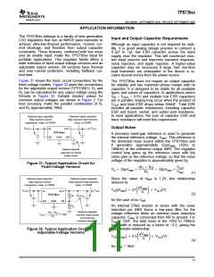
After the enable pin is driven low, no bias voltage is
needed on any pin for reverse current blocking. Note
that reverse current is specified as the current flowing
out of the IN pin due to voltage applied on the OUT
pin. There will be additional current flowing into the
OUT pin due to the 80kΩ internal resistor divider to
ground (see Figure 1 and Figure 2).
For the TPS73601, reverse current may flow when
VFB is more than 1.0V above VIN.
Power dissipation depends on input voltage and load
conditions. Power dissipation is equal to the product
of the output current times the voltage drop across
the output pass element (VIN to VOUT):
Thermal Protection
Thermal protection disables the output when the
junction temperature rises to approximately 160°C,
allowing the device to cool. When the junction tem-
perature cools to approximately 140°C, the output
circuitry is again enabled. Depending on power dissi-
pation, thermal resistance, and ambient temperature,
the thermal protection circuit may cycle on and off.
This limits the dissipation of the regulator, protecting
it from damage due to overheating.
PD
(VIN VOUT
)
IOUT
(6)
Power dissipation can be minimized by using the
lowest possible input voltage necessary to assure the
required output voltage.
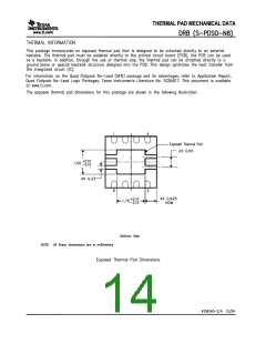
Package Mounting
Any tendency to activate the thermal protection circuit
indicates excessive power dissipation or an inad-
equate heat sink. For reliable operation, junction
temperature should be limited to 125°C maximum. To
estimate the margin of safety in a complete design
(including heat sink), increase the ambient tempera-
ture until the thermal protection is triggered; use
worst-case loads and signal conditions. For good
reliability, thermal protection should trigger at least
35°C above the maximum expected ambient con-
dition of your application. This produces a worst-case
junction temperature of 125°C at the highest
Solder pad footprint recommendations for the
TPS736xx are presented in Application Bulletin
Solder Pad Recommendations for Surface-Mount De-
vices (AB-132), available from the Texas Instruments
web site at www.ti.com.
13

 TI [ TEXAS INSTRUMENTS ]