TPS736xx
www.ti.com
SBVS038K–SEPTEMBER 2003–REVISED SEPTEMBER 2005
This noise reduction effect is shown as RMS Noise
Voltage vs CNR in the Typical Characteristics section.
For large step changes in load current, the TPS736xx
requires a larger voltage drop from VIN to VOUT to
avoid degraded transient response. The boundary of
this transient dropout region is approximately twice
the dc dropout. Values of VIN - VOUT above this line
insure normal transient response.
The TPS73601 adjustable version does not have the
noise-reduction pin available. However, connecting a
feedback capacitor, CFB , from the output to the FB
pin will reduce output noise and improve load transi-
ent performance.
Operating in the transient dropout region can cause
an increase in recovery time. The time required to
recover from a load transient is a function of the
magnitude of the change in load current rate, the rate
of change in load current, and the available head-
room (VIN to VOUT voltage drop). Under worst-case
conditions [full-scale instantaneous load change with
(VIN - VOUT) close to dc dropout levels], the TPS736xx
can take a couple of hundred microseconds to return
to the specified regulation accuracy.
The TPS736xx uses an internal charge pump to
develop an internal supply voltage sufficient to drive
the gate of the NMOS pass element above VOUT. The
charge pump generates ~250µV of switching noise at
~4MHz; however, charge-pump noise contribution is
negligible at the output of the regulator for most
values of IOUT and COUT
.
Board Layout Recommendation to Improve
PSRR and Noise Performance
Transient Response
To improve ac performance such as PSRR, output
noise, and transient response, it is recommended that
the board be designed with separate ground planes
for VIN and VOUT, with each ground plane connected
only at the GND pin of the device. In addition, the
ground connection for the bypass capacitor should
connect directly to the GND pin of the device.
The low open-loop output impedance provided by the
NMOS pass element in a voltage follower configur-
ation allows operation without an output capacitor for
many applications. As with any regulator, the addition
of a capacitor (nominal value 1µF) from the output pin
to ground will reduce undershoot magnitude but
increase duration. In the adjustable version, the
addition of a capacitor, CFB, from the output to the
adjust pin will also improve the transient response.
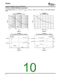
Internal Current Limit
The TPS736xx internal current limit helps protect the
regulator during fault conditions. Foldback helps to
protect the regulator from damage during output
short-circuit conditions by reducing current limit when
VOUT drops below 0.5V. See Figure 11 in the Typical
The TPS736xx does not have active pull-down when
the output is over-voltage. This allows applications
that connect higher voltage sources, such as alter-
nate power supplies, to the output. This also results
in an output overshoot of several percent if load
current quickly drops to zero when a capacitor is
connected to the output. The duration of overshoot
can be reduced by adding a load resistor. The
overshoot decays at a rate determined by output
capacitor COUT and the internal/external load resist-
ance. The rate of decay is given by:
Characteristics section for a graph of IOUT vs VOUT
.
Shutdown
The Enable pin is active high and is compatible with
standard TTL-CMOS levels. VEN below 0.5V (max)
turns the regulator off and drops the ground pin
current to approximately 10nA. When shutdown capa-
bility is not required, the Enable pin can be connected
to VIN. When a pull-up resistor is used, and operation
down to 1.8V is required, use pull-up resistor values
below 50kΩ.
(Fixed Voltage Version)
VOUT
dVńdt +
COUT 80kW ø RLOAD
(4)
(Adjustable Voltage Version)
VOUT
dVńdt +
Dropout Voltage
(
)
COUT 80kW ø R1 ) R2 ø RLOAD
(5)
The TPS736xx uses an NMOS pass transistor to
achieve extremely low dropout. When (VIN - VOUT) is
less than the dropout voltage (VDO), the NMOS pass
device is in its linear region of operation and the
input-to-output resistance is the RDS-ON of the NMOS
pass element.
12

 TI [ TEXAS INSTRUMENTS ]