TPS61196
www.ti.com
SLVSBG1C –OCTOBER 2012–REVISED FEBRUARY 2013
2IOUT
fP
=
2πVOUT ´ COUT
(12)
(13)
2
VOUT ´ 1-D
(
2πL ´ IOUT
)
fZRHP
=
To make the loop stable, the loop must have sufficient phase margin at the crossover frequency where the loop
gain is 1. To avoid the effect of the right half plane zero on the loop stability, choose the crossover frequency
less than 1/5 of the fZRHP. Then calculate the compensation components by Equation 14 and Equation 15.
R7 ´2πfco ´COUT
VOVP
R8 =
´
1-D ´ Gm
)
VOVPTH
(
EA
(14)
Where VOVPTH = 3.02V, which is the internal reference for the output over-voltage-protection setting voltage. VOVP
is the output over-voltage-protection setting voltage. GmEA is the trans-conductance of the error amplifier. Its
typical value is 120μS. fCO is the crossover frequency, which normally is less than 1/5 of the fZRHP
.
1
C6 =
2πfP ´ R8
(15)
Where fP is the pole’s frequency of the power stage calculated by Equation 12. If the output cap is the electrolytic
capacitor which may have large ESR, a capacitor is required to cancel the zero of the output capacitor.
Equation 16 calculates the value of this capacitor.
COUT ´ RESR
C8 =
R8
(16)
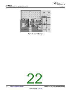
Layout Consideration
As for all switching power supplies, especially those providing high current and using high switching frequencies,
layout is an important design step. If layout is not carefully done, the regulator could show instability as well as
EMI problems. Therefore, use wide and short traces for high current paths. The VDD capacitor, C3 (see in
SIMPLIFIED SCHEMATIC CIRCUIT) is the filter and noise decoupling capacitor for the internal linear regulator
powering the internal digital circuits. It should be placed as close as possible between the VDD and PGND pins
to prevent any noise insertion to digital circuits. The switch node at the drain of Q1 carries high current with fast
rising and falling edges. Therefore, the connection between this node to the inductor and the schottky diode
should be kept as short and wide as possible. It is also beneficial to have the ground of the capacitor C3 close to
the ground of the current sense resistor R7 since there is large driving current flowing between them. The ground
of output capacitor EC2 should be kept close to input power ground or through a large ground plane because of
the large ripple current returning to the input ground. When laying out signal grounds, it is recommended to use
short traces separate from power ground traces and connect them together at a single point, for example on the
thermal pad in the PWP package. Resistors R3, R4, R9, R10, R11 and R12 (see in the SIMPLIFIED
SCHEMATIC CIRCUIT) are setting resistors for switching frequency, LED current, protection threshold and
feedback voltage programming. To avoid unexpected noise coupling into the pins and affecting the accuracy,
these resistors need to be close to the pins with short and wide traces to GND. In PWP package, the thermal
pad needs to be soldered to the large ground plane on the PCB for better thermal performance. Additional
thermal via can significantly improve power dissipation of the IC.
Copyright © 2012–2013, Texas Instruments Incorporated
Submit Documentation Feedback
21
Product Folder Links :TPS61196

 TI [ TEXAS INSTRUMENTS ]