TPS56528
www.ti.com
SLVSBV3A –APRIL 2013–REVISED APRIL 2013
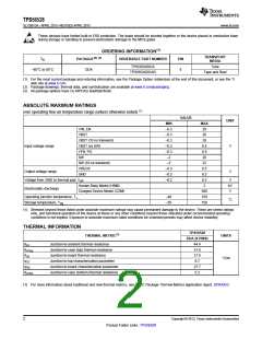
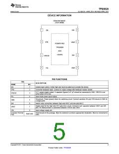
DEVICE INFORMATION
DDA PACKAGE
(TOP VIEW)
8
1
VIN
EN
2
7
VFB
VBST
POWER PAD
TPS56528
DDA
HSOP8
3
6
SW
VREG5
4
5
GND
PG
PIN FUNCTIONS
PIN
DESCRIPTION
NAME
EN
NO.
1
Enable input control. Active high and must be pulled up to enable the device.
Converter feedback input. Connect to output voltage with feedback resistor divider.
VFB
2
5.5 V power supply output. A capacitor (typical 0.47 µF) should be connected to GND. VREG5 is not
active when EN is low.
VREG5
PG
3
4
Open drain power good output.
Ground pin. Power ground return for switching circuit. Connect sensitive SS and VFB returns to GND at
a single point.
GND
SW
5
6
Switch node connection between high-side NFET and low-side NFET.
Supply input for the high-side FET gate drive circuit. Connect 0.1µF capacitor between VBST and SW
pins. An internal diode is connected between VREG5 and VBST.
VBST
VIN
7
8
Input voltage supply pin.
Exposed Thermal
Pad
Thermal pad of the package. Must be soldered to achieve appropriate dissipation. Must be connected to
GND.
Back side
Copyright © 2013, Texas Instruments Incorporated
5
Product Folder Links :TPS56528

 TI [ TEXAS INSTRUMENTS ]