TPS562212
ZHCSNA3 –OCTOBER 2021
www.ti.com.cn
V
- VOUT
VOUT
IN_MAX
IRIPPLE
=
∂
V
L1 ∂ fSW
IN_MAX
(13)
(14)
IRIPPLE
ILPEAK = IOUT
+
2
1
2
2
ILRMS
=
IOUT
+
IRIPPLE
12
(15)
For this design example, the calculated peak current is 2.68 A and the calculated RMS current is 2.04 A. The
chosen inductor is a Wurth Elektronik 74439344022 2.2-μH. It has a saturation current rating of 16 A and a
RMS current rating of 8 A.
The current flowing through the inductor is the inductor ripple current plus the output current. During power up,
faults, or transient load conditions, the inductor current can increase above the calculated peak inductor current
level calculated above. In transient conditions, the inductor current can increase up to the switch current limit of
the device. For this reason, the most conservative approach is to specify an inductor with a saturation current
rating equal to or greater than the switch current limit rather than the peak inductor current.
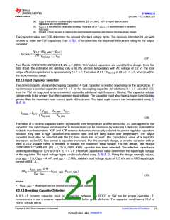
8.2.2.4 Output Capacitor Selection
After selecting the inductor, the output capacitor needs to be optimized. The LC filter used as the output filter has
double pole at:
1
fP =
2p L1 ∂COUT _E
(16)
At low frequencies, the overall loop gain is set by the output set-point resistor divider network and the internal
gain of the device. The low frequency phase is 180°. At the output filter pole frequency, the gain rolls off at a –
40 dB per decade rate and the phase drops rapidly. A high frequency zero is introduced by the internal circuit
that reduces the gain roll off to –20 dB per decade and increases the phase to 90° one decade above the zero
frequency. The inductor and capacitor for the output filter must be selected so that the double pole of fP is
located below the high frequency zero, but close enough. The phase boost provided by the high frequency zero
provides adequate phase margin for a stable circuit. To meet this requirement, it is better to make the L1 ×
COUT_E value meet the range of the L1 × COUT_E value recommended in 表8-2.
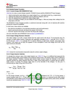
表8-2. Recommended Component Values
RANGE OF L1 ×
R8(2)
(kΩ)
R9
(kΩ)
(4)
OUTPUT
L1(3)
(µH)
COUT
(µF)
C7(6)
(pF)
(5)
COUT_E
VOLTAGE (V)(1)
(μH × μF)
17–130
17–130
15–160
15–160
15–160
15–160
0.76
1.05
1.8
2.5
3.3
5
5.36
15.0
40.0
31.6
45.3
73.2
20.0
20.0
20.0
10.0
10.0
10.0
0.68
1.0
1.5
1.8
2.2
3.3
2 × 22
2 × 22
1 × 22
1 × 22
1 × 22
1 × 22
—
10–100
10–100
10–100
10–100
10–100
(1) Use the recommended L1 and COUT combination of the higher and closest output rail for the
unlisted output rails.
(2) R8 = 10 kΩand R9 = Float for VOUT = 0.6 V
(3) Inductance values are calculated based on VIN=18 V, but they can also be used for other input
voltages. Users can calculate their preferred inductance value per 方程式12.
Copyright © 2021 Texas Instruments Incorporated
20
Submit Document Feedback
Product Folder Links: TPS562212

 TI [ TEXAS INSTRUMENTS ]