TPS562212
ZHCSNA3 –OCTOBER 2021
www.ti.com.cn
8.2.2 Detailed Design Procedure
8.2.2.1 Custom Design With WEBENCH® Tools
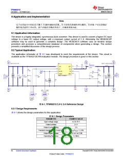
Click here to create a custom design using the TPS562212 device with the WEBENCH® Power Designer.
1. Start by entering the input voltage (VIN), output voltage (VOUT), and output current (IOUT) requirements.
2. Optimize the design for key parameters such as efficiency, footprint, and cost.
3. Open the advanced tab to optimize for output voltage ripple.
4. Once in a TPS562212 design, you can enable the second stage L-C filter and change other settings from the
drop-down on the left.
The WEBENCH Power Designer provides a customized schematic along with a list of materials with real-time
pricing and component availability.
In most cases, these actions are available:
• Run electrical simulations to see important waveforms and circuit performance
• Export customized schematic and layout into popular CAD formats
• Print PDF reports for the design, and share the design with colleagues
Get more information about WEBENCH tools at www.ti.com/WEBENCH.
8.2.2.2 Output Voltage Resistors Selection
The output voltage is set with a resistor divider from the output node to the FB pin. TI recommends using 1%
tolerance or better divider resistors. Referring to the application schematic of 图 8-1, start with 10 kΩ or 20 kΩ
for R9 and use 方程式 11 to calculate R8. To improve efficiency at light loads, consider using larger value
resistors. If the values are too high, the regulator is more susceptible to noise and voltage errors from the FB
input current are noticeable.
VOUT - VREF
VREF
R8 =
∂R9
(11)
表8-2 shows the recommended components value for common output voltages.
8.2.2.3 Output Inductor Selection
To calculate the minimum value of the output inductor, use 方程式 12. KIND is a coefficient that represents the
amount of inductor ripple current relative to the maximum output current. The inductor ripple current is filtered by
the output capacitor. Therefore, choosing high inductor ripple currents impact the selection of the output
capacitor because the output capacitor must have a ripple current rating equal to or greater than the inductor
ripple current. In general, the inductor ripple value is at the discretion of the designer. For this part, TI
recommends the range of KIND from 25% to 55%.
V
- VOUT
VOUT
IN_MAX
LMIN
=
∂
V
KIND ∂IOUT ∂ fSW
IN_MAX
(12)
where
• IOUT = 2 A
For this design example, use KIND = 50%. The inductor value is calculated to be 2.25 μH. For this design, a
nearest standard value of 2.2 μH was chosen. For the output filter inductor, it is important that the RMS current
and saturation current ratings not be exceeded. The inductor peak-to-peak ripple current, peak current, and RMS
current are calculated using 方程式13, 方程式14, and 方程式15.
Copyright © 2021 Texas Instruments Incorporated
Submit Document Feedback
19
Product Folder Links: TPS562212

 TI [ TEXAS INSTRUMENTS ]