ꢀ
ꢁ
ꢂ
ꢃ
ꢄ
ꢅ
ꢆ
ꢇ
www.ti.com
SLVS398D − JUNE 2001 − REVISED JULY 2003
APPLICATION INFORMATION
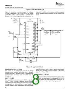
Figure 10 shows the schematic diagram for a typical
TPS54610 application. The TPS54610 (U1) can provide
greater than 6 A of output current at a nominal output
voltage of 3.3 V. For proper thermal performance, the
exposed thermal PowerPAD underneath the integrated
circuit package must be soldered to the printed-circuit
board.
V
I
C2
220 µF
10 V
U1
+
C8
TPS54610PWP
10 µF
28
24
RT
VIN
R2
23
22
21
VIN
VIN
VIN
VIN
PH
PH
PH
PH
PH
PH
PH
PH
10 kΩ
27
26
SYNC
SS/ENA
L1
4.7 µH
20
14
13
V
O
25
C9
470 µF
4 V
C10
470 µF
4 V
C11
100 pF
+
+
VBIAS
PWRGD
COMP
C1
0.047 µF
12
11
PWRGD
4
3
10
9
C4
0.1 µF
8
7
6
C7
PH
BOOT
PGND
PGND
2
1
5
VSENSE
AGND
19
18
17
16
15
0.047 µF
PGND
PGND
PGND
C5
5600 pF
C3
120 pF
POWERPAD
R1
9.09 kΩ
C6
R5
1.74 kΩ
8200 pF
R3
3.74 kΩ
R4
10 kΩ
Figure 10. Application Circuit
current is carried in both C2 and C8, and the return path to
PGND must avoid the current circulating in the output
capacitors C9 and C10.
COMPONENT SELECTION
The values for the components used in this design
example were selected using the SWIFT designer
software tool. SWIFT designer provides a complete design
environment for developing dc-dc converters using the
TPS54610.
FEEDBACK CIRCUIT
The resistor divider network of R3 and R4 sets the output
voltage for the circuit at 3.3 V. R4, along with R1, R5, C3,
C5, and C6 form the loop compensation network for the
circuit. For this design, a Type 3 topology is used.
INPUT FILTER
The input to the circuit is a nominal 5 VDC. The input filter
C2 is a 220-µF POSCAP capacitor, with a maximum
allowable ripple current of 3 A. C8 provides high frequency
decoupling of the TPS54610 from the input supply and
must be located as close as possible to the device. Ripple
8

 TI [ TEXAS INSTRUMENTS ]